Samsung Extends Its DRAM Market Lead
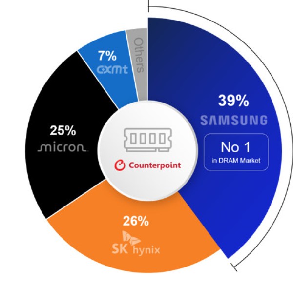
DRAM prices and supplier concentration can directly reshape the cost and availability of AI infrastructure.
30-Second TL;DR
What Changed
Samsung ranked first in the global DRAM market for three consecutive quarters.
Why It Matters
DRAM leadership and pricing trends matter to AI infrastructure because memory availability and cost affect server procurement and accelerator deployments. A widening supplier gap may also influence sourcing strategies for data-center operators and AI hardware builders.
What To Do Next
Recheck your AI server bill of materials and request updated Samsung DRAM pricing and lead-time quotes before committing to the next deployment batch.
Key Points
- •Samsung ranked first in the global DRAM market for three consecutive quarters.
- •Counterpoint reported that DRAM memory prices continued to rise during the second quarter.
- •Samsung was identified as the biggest beneficiary of the price increase.
- •The company widened its lead over SK Hynix.
Deep Insight
AI-generated analysis for this event — not the original article.
Enhanced Key Takeaways
- •The DRAM market recovery is largely driven by the surge in demand for High Bandwidth Memory (HBM) used in AI accelerators and generative AI infrastructure.
- •Samsung has been aggressively transitioning its production capacity toward HBM3E and HBM4 to capture higher margins compared to legacy DDR4 and DDR5 modules.
- •SK Hynix maintains a dominant position specifically in the HBM market, despite Samsung's overall DRAM revenue lead, due to early partnerships with major AI chip designers.
- •Micron Technology has emerged as a critical third player, successfully ramping up its 1-beta and 1-gamma node production to compete in the high-density DRAM segment.
- •Inventory normalization across PC and smartphone sectors has concluded, leading to a more stable supply-demand balance that supports sustained average selling price (ASP) growth.
Competitor Analysis
- Samsung
- HBM3E / HBM4
- SK Hynix
- HBM3E (Market Leader)
- Micron
- HBM3E (High Capacity)
- Samsung
- 12nm-class (1b)
- SK Hynix
- 10nm-class (1b/1c)
- Micron
- 1-beta / 1-gamma
- Samsung
- Vertical Integration
- SK Hynix
- AI-Centric Specialization
- Micron
- Cost-Efficiency & Density
| Feature | Samsung | SK Hynix | Micron |
|---|---|---|---|
| Primary HBM Focus | HBM3E / HBM4 | HBM3E (Market Leader) | HBM3E (High Capacity) |
| Process Node | 12nm-class (1b) | 10nm-class (1b/1c) | 1-beta / 1-gamma |
| Market Strategy | Vertical Integration | AI-Centric Specialization | Cost-Efficiency & Density |
Technical Deep Dive
- Samsung is utilizing 12nm-class (1b) process technology to enhance power efficiency and density for its latest DRAM offerings.
- The company is implementing EUV (Extreme Ultraviolet) lithography across multiple layers to achieve the precision required for high-speed HBM3E stacks.
- Advanced packaging techniques, specifically TC-NCF (Thermal Compression Non-Conductive Film), are being deployed to manage thermal dissipation in high-stack HBM configurations.
- Samsung's roadmap includes the integration of CXL (Compute Express Link) 3.0 technology to enable memory pooling and expansion for data center workloads.
Future ImplicationsAI analysis grounded in cited sources
Timeline
- 2023-05Samsung announces the development of its first 12nm-class DDR5 DRAM.
- 2024-02Samsung unveils the industry's first 36GB HBM3E 12-layer DRAM.
- 2024-10Samsung begins mass production of 12-layer HBM3E memory.
- 2025-06Samsung reports record DRAM revenue growth driven by AI server demand.
- 2026-04Samsung maintains global DRAM market share lead for the first quarter of 2026.
Weekly AI Recap
Read this week's curated digest of top AI events →
Related Updates

AI-curated news aggregator. All content rights belong to original publishers.
Original source: cnBeta (Full RSS) ↗
This is a summary, not the original. Read the source, or get the weekly briefing.
The weekly digest
One email a week. Unsubscribe anytime.