Samsung & SK Hynix Ramp China Investments
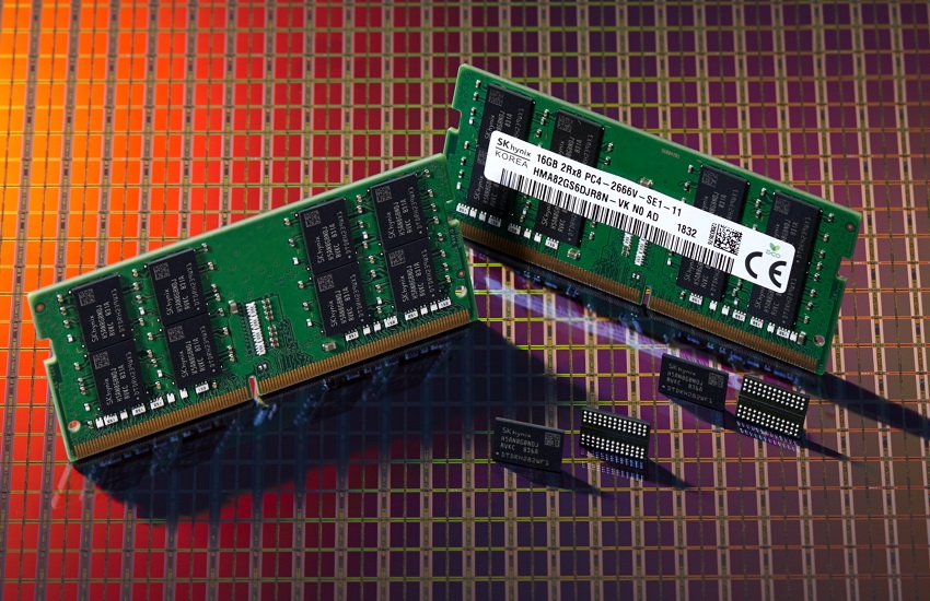
💡Memory expansion fixes AI data center supply crunch
⚡ 30-Second TL;DR
What Changed
Samsung and SK Hynix to expand China investments in 2025
Why It Matters
Expansion eases memory shortages vital for AI training clusters and GPU servers, potentially lowering costs for AI infrastructure builds. Strengthens China-dependent supply chains for global AI hardware.
What To Do Next
Track Samsung HBM supply announcements for AI GPU procurement planning.
Key Points
- •Samsung and SK Hynix to expand China investments in 2025
- •Focus on increasing factory capacity for storage chips
- •Upgrading manufacturing processes to address shortages
- •Response to global memory market supply-demand imbalance
🧠 Deep Insight
AI-generated analysis for this event — not the original article.
🔑 Enhanced Key Takeaways
- •The expansion is heavily focused on advanced NAND flash production, specifically targeting the transition to 200+ layer 3D NAND nodes to maintain cost competitiveness against domestic Chinese rivals like YMTC.
- •These investments are navigating complex US export controls, requiring Samsung and SK Hynix to secure 'Validated End-User' (VEU) status to import advanced lithography equipment into their Chinese facilities.
- •The strategy reflects a shift toward 'local-for-local' production, aiming to supply the rapidly growing Chinese EV and AI server markets directly from within the country to mitigate geopolitical supply chain risks.
📊 Competitor Analysis▸ Show
| Feature | Samsung (China) | SK Hynix (China) | YMTC (China) | Micron (US/Global) |
|---|---|---|---|---|
| Primary Focus | High-end NAND/DRAM | High-end DRAM | 3D NAND | High-end DRAM/NAND |
| Tech Node | 200+ Layer NAND | Advanced DRAM | 232+ Layer NAND | 200+ Layer NAND |
| Geopolitical Risk | High (US/China) | High (US/China) | Low (Domestic) | Moderate (China ban) |
🛠️ Technical Deep Dive
- •Transitioning from 176-layer to 236-layer and 300-layer class 3D NAND architectures to increase bit density per wafer.
- •Implementation of EUV (Extreme Ultraviolet) lithography for DRAM production in China, subject to strict US licensing requirements for equipment maintenance and upgrades.
- •Utilization of high-aspect-ratio etching processes to enable deeper channel holes for higher-layer-count NAND stacks.
- •Integration of advanced packaging technologies (e.g., hybrid bonding) to improve data transfer speeds and power efficiency in memory modules.
🔮 Future ImplicationsAI analysis grounded in cited sources
⏳ Timeline
Weekly AI Recap
Read this week's curated digest of top AI events →
👉Related Updates


AI-curated news aggregator. All content rights belong to original publishers.
Original source: cnBeta (Full RSS) ↗
This is a summary, not the original. Read the source, or get the weekly briefing.
Weekly AI briefing
One email a week. Unsubscribe anytime.