🇨🇳cnBeta (Full RSS)•Stalecollected in 2h
Rapidus Activates Advanced Packaging Pilot Line

💡Rapidus chiplet packaging pilot live—key enabler for Japan's AI chip ambitions.
⚡ 30-Second TL;DR
What Changed
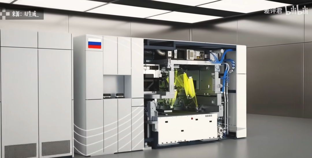
Pilot line officially enabled in Hokkaido Chitose
Why It Matters
Accelerates Japan's chiplet ecosystem for next-gen logic chips, vital for scalable AI hardware like multi-chiplet GPUs. Reduces reliance on foreign advanced packaging tech.
What To Do Next
Test Rapidus RDL interposers in chiplet-based AI accelerator prototypes for 2nm designs.
Who should care:Researchers & Academics
🧠 Deep Insight
AI-generated analysis for this event.
🔑 Enhanced Key Takeaways
- •The pilot line utilizes a 'Chiplet-on-Wafer-on-Substrate' (CoWoS)-like architecture, specifically targeting the integration of 2nm logic chips with high-bandwidth memory (HBM) to meet the demands of generative AI hardware.
- •Rapidus is leveraging a strategic partnership with IBM for 2nm process technology, which is being integrated into the packaging workflow to ensure high-yield interconnects between the logic die and the RDL interposer.
- •The Chitose facility is designed to serve as a 'foundry-plus-packaging' ecosystem, aiming to reduce the total cycle time for advanced semiconductor manufacturing by keeping the packaging process in close proximity to the wafer fabrication site.
📊 Competitor Analysis▸ Show
| Feature | Rapidus (Hokkaido) | TSMC (CoWoS) | Intel (Foveros) |
|---|---|---|---|
| Primary Focus | 2nm Logic + Chiplet | Advanced Packaging Ecosystem | 3D Stacking / Hybrid Bonding |
| Interposer Tech | 600mm x 600mm RDL | Silicon / Organic Interposers | Embedded Multi-die Interconnect |
| Market Position | Emerging / Sovereign | Dominant / High-Volume | Integrated / IDM 2.0 |
🛠️ Technical Deep Dive
- Interposer Technology: Utilizes large-format 600mm x 600mm Redistribution Layer (RDL) interposers to facilitate high-density signal routing between chiplets.
- Integration Strategy: Employs advanced bonding techniques to support high-speed data transfer between 2nm logic dies and HBM stacks.
- Facility Infrastructure: The pilot line is integrated within Seiko Epson’s existing cleanroom infrastructure, optimized for high-precision alignment required for chiplet assembly.
- Process Node: Specifically engineered to support the thermal and electrical requirements of 2nm-class logic chips.
🔮 Future ImplicationsAI analysis grounded in cited sources
Rapidus will achieve mass production of 2nm chiplet-based AI accelerators by 2027.
The successful activation of the pilot line provides the necessary infrastructure to transition from R&D to high-volume manufacturing within the company's stated timeline.
The Hokkaido facility will reduce Japan's reliance on overseas advanced packaging services by at least 30% for domestic AI chip production.
By localizing the packaging process, Rapidus eliminates the need to ship wafers to third-party providers in Taiwan or Southeast Asia, shortening the supply chain.
⏳ Timeline
2022-11
Rapidus Corporation is established with support from the Japanese government and major industry partners.
2023-02
Rapidus announces a strategic partnership with IBM to license 2nm semiconductor manufacturing technology.
2023-09
Rapidus selects Chitose, Hokkaido, as the site for its IIM-1 (Integrated Innovation Manufacturing) fab.
2024-04
Construction begins on the main Rapidus fabrication facility in Chitose.
2026-04
Rapidus officially activates the advanced packaging pilot line at the Seiko Epson factory.
📰
Weekly AI Recap
Read this week's curated digest of top AI events →
👉Related Updates

AI-curated news aggregator. All content rights belong to original publishers.
Original source: cnBeta (Full RSS) ↗