NVIDIA Feynman GPU: 1.6nm, 1000W+ Debut
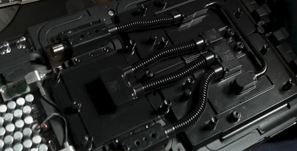
💡NVIDIA's 1.6nm Feynman GPU eyes 1000W+ AI compute leap at GTC – infra game-changer.
⚡ 30-Second TL;DR
What Changed
GTC announcement scheduled for March 16-19
Why It Matters
Feynman's extreme power and advanced node could accelerate large-scale AI training but strain data center infrastructure with cooling and energy demands.
What To Do Next
Register for NVIDIA GTC 2025 livestream starting March 16 to evaluate Feynman for your AI cluster builds.
Key Points
- •GTC announcement scheduled for March 16-19
- •First use of 1.6nm process node
- •Power consumption over 1000W TDP
- •Integrates next-gen HBM memory
- •Named after physicist Richard Feynman
🧠 Deep Insight
Background and context from public sources — not the original article. 8 sources cited.
🔑 Enhanced Key Takeaways
- •Feynman architecture follows NVIDIA's Blackwell and Rubin successors, with mass production and launch projected for 2028[1][2].
- •Built on TSMC's A16 (1.6nm-class) node featuring Super Power Rail (SPR) technology, with potential partial outsourcing of I/O die production to Intel[1][2][7].
- •Pairs with HBM4 memory supplied by Samsung and SK Hynix, already in mass production for NVIDIA's Rubin GPUs[1][2].
- •Engineered for real-time agentic AI workloads, enabling autonomous systems like robotics and on-device decision-making[6].
🛠️ Technical Deep Dive
- •Utilizes TSMC A16 node (1.6nm-class) with Super Power Rail (SPR) for enhanced power delivery[7].
- •Incorporates silicon photonics for optical interconnects in rack-scale compute units[2].
- •Potential Intel outsourcing for I/O die on 14A/18A processes and EMIB advanced packaging to mitigate TSMC capacity risks[2].
- •Optimized for agentic AI, shifting from training-focused compute to real-time inference and decision-making[6].
🔮 Future ImplicationsAI analysis grounded in cited sources
⏳ Timeline
📎 Sources (8)
Factual claims are grounded in the sources below. Forward-looking analysis is AI-generated interpretation.
- technetbooks.com — Nvidia Feynman AI Architecture Will
- trendforce.com — News Nvidia Gtc 2026 in Focus Feynman Reportedly on TSMC A16 Samsung Sk Hynix to Showcase Hbm4
- theregister.com — Nvidia Gtc 2026 Preview Tobias Mann Register
- longbridge.com — 278246493
- fundaai.substack.com — Deepgtc 2026 Preview Nvidia Is Rewriting
- ainvest.com — Nvidia Gtc 2026 Reveal Feynman AI Chip Infrastructure Curve Inflection 2603
- hwbusters.com — Nvidia May Unveil First 1 6nm Feynman Chips at Gtc 2026
- markets.financialcontent.com — Marketminute 2026 3 11 Nvidia Gtc 2026 the World Surprising Chip and the Dawn of the Agentic AI Era
Weekly AI Recap
Read this week's curated digest of top AI events →
👉Related Updates
AI-curated news aggregator. All content rights belong to original publishers.
Original source: cnBeta (Full RSS) ↗
This is a summary, not the original. Read the source, or get the weekly briefing.
Weekly AI briefing
One email a week. Unsubscribe anytime.