Naura Advances Two-Step Etching for 3D DRAM
💡A new 3D DRAM etching route could reshape memory supply options for AI infrastructure.
⚡ 30-Second TL;DR
What Changed
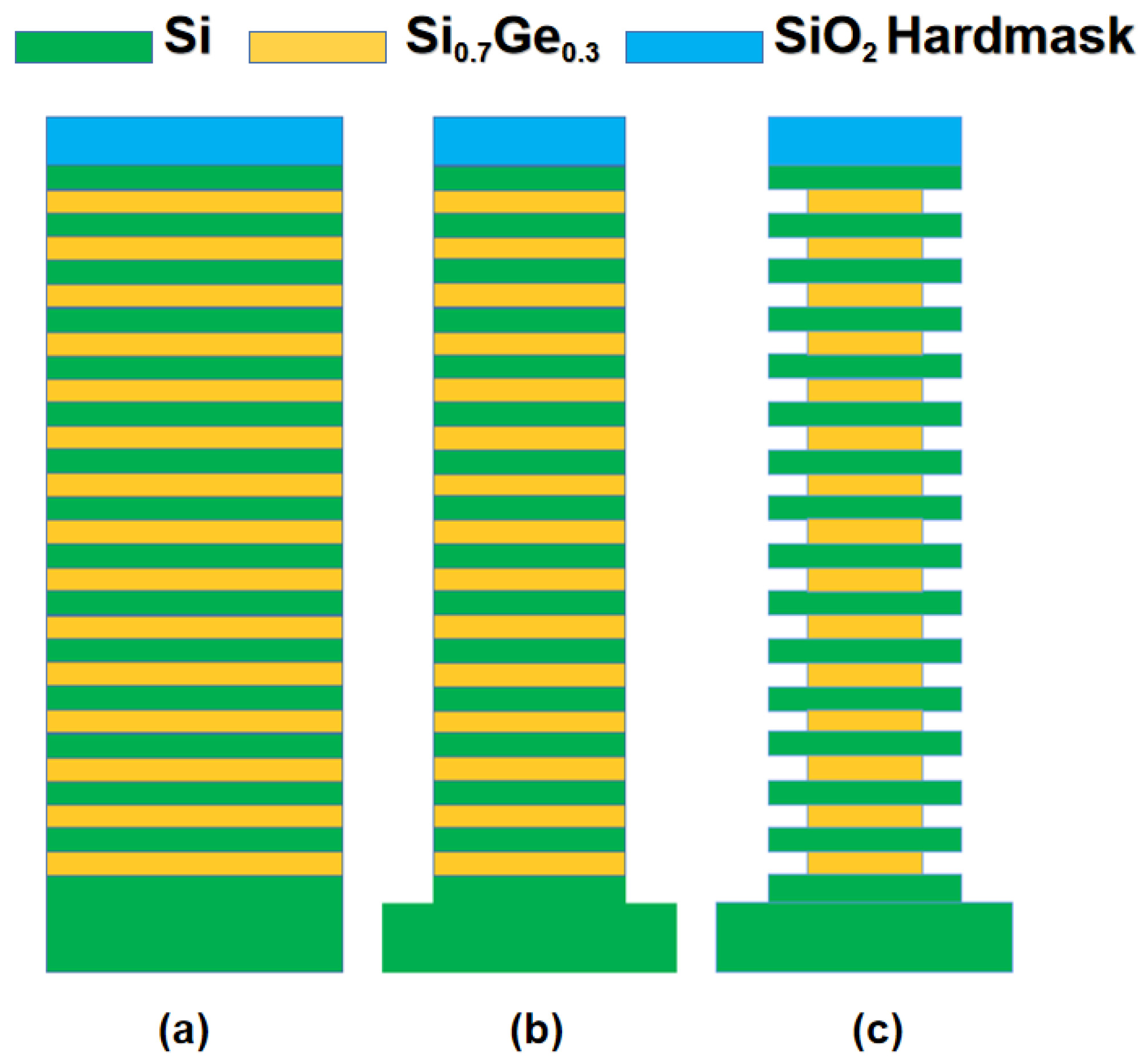
Naura reported a two-step cyclic etching process for 3D DRAM fabrication.
Why It Matters
If the process can be transferred to high-volume manufacturing, it may improve China’s ability to develop denser memory without direct access to the most advanced EUV tools. For AI infrastructure companies, greater domestic DRAM capability could eventually broaden memory sourcing options, although production readiness is not yet established.
What To Do Next
For AI infrastructure planning, ask memory suppliers for validated 3D DRAM roadmaps, process-yield data, and EUV dependency before revising procurement assumptions.
Key Points
- •Naura reported a two-step cyclic etching process for 3D DRAM fabrication.
- •The technology targets higher transistor density through vertical chip stacking.
- •The process could provide CXMT and other Chinese memory firms with an alternative path amid EUV export controls.
Weekly AI Recap
Read this week's curated digest of top AI events →
👉Related Updates


AI-curated news aggregator. All content rights belong to original publishers.
Original source: cnBeta (Full RSS) ↗
This is a summary, not the original. Read the source, or get the weekly briefing.
Weekly AI briefing
One email a week. Unsubscribe anytime.