Musk's Terafab Could Become Earth's Largest Building
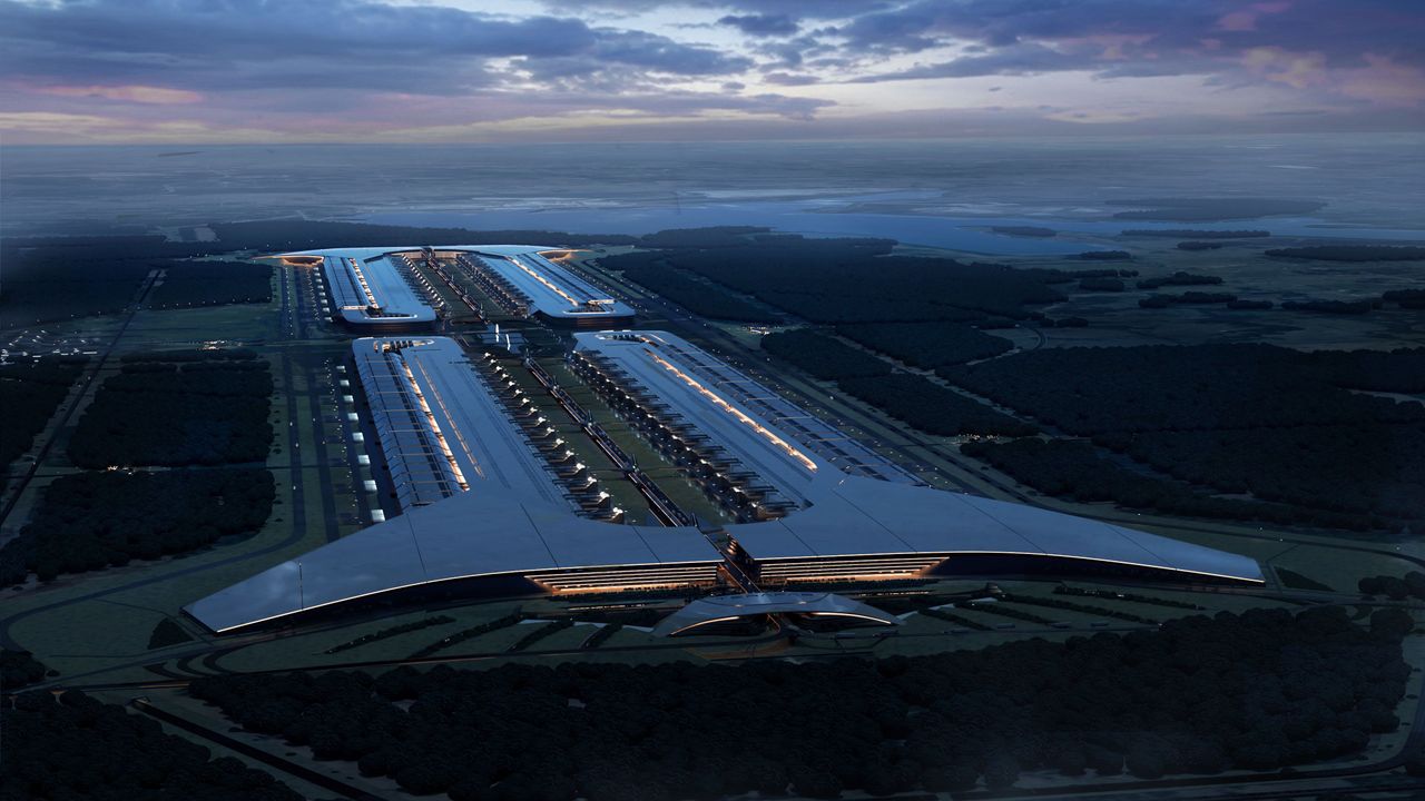
A proposed chip megafactory could reshape how AI hardware capacity is built and integrated.
30-Second TL;DR
What Changed
The projected facility would contain at least 100 million square feet of interior space.
Why It Matters
If realized, Terafab could represent an unusually aggressive attempt to vertically integrate chip production for AI and other compute-heavy systems. The enormous scale also highlights the capital, energy, and supply-chain demands of expanding advanced computing infrastructure.
What To Do Next
Add the Terafab projection to your AI infrastructure roadmap and stress-test future accelerator capacity plans against its 100-million-square-foot assumption.
Key Points
- •The projected facility would contain at least 100 million square feet of interior space.
- •Its footprint is described as larger than the Pentagon, Apple Park, Mall of America, and Giga Texas combined.
- •The plan aims to consolidate multiple semiconductor manufacturing processes in one facility.
Deep Insight
AI-generated analysis for this event — not the original article.
Enhanced Key Takeaways
- •The Terafab concept is intrinsically linked to Tesla's 'Master Plan Part 3,' which emphasizes the massive scaling of manufacturing infrastructure required for a sustainable energy economy.
- •Industry analysts suggest the facility is designed to utilize 'first-principles' engineering to integrate raw material processing, component fabrication, and final assembly into a continuous, automated flow.
- •The facility is expected to leverage Tesla's proprietary 'Unboxed' manufacturing process, which reduces factory footprint while increasing production efficiency by assembling vehicle sections in parallel.
- •Energy requirements for a facility of this magnitude are projected to be met through on-site, massive-scale solar arrays and integrated battery energy storage systems (BESS).
- •The project aims to mitigate supply chain volatility by vertically integrating the production of critical semiconductor components and power electronics directly within the manufacturing ecosystem.
Technical Deep Dive
- Implementation of high-degree automation utilizing AI-driven robotics for material handling and assembly line optimization.
- Integration of vertical manufacturing stacks to minimize horizontal floor space usage while maximizing throughput.
- Utilization of advanced thermal management systems designed to handle the high heat loads generated by concentrated semiconductor fabrication processes.
- Modular facility design allowing for rapid scaling and reconfiguration of production lines without halting overall operations.
Future ImplicationsAI analysis grounded in cited sources
Timeline
- 2023-03Tesla Investor Day presentation outlines the 'Master Plan Part 3' and the vision for massive-scale, integrated manufacturing.
- 2023-03Introduction of the 'Unboxed' manufacturing process concept during Tesla's Investor Day.
- 2024-05Reports emerge regarding Tesla's exploration of massive, consolidated manufacturing sites to support future product scaling.
Weekly AI Recap
Read this week's curated digest of top AI events →
AI-curated news aggregator. All content rights belong to original publishers.
Original source: Tom's Hardware ↗
This is a summary, not the original. Read the source, or get the weekly briefing.
The weekly digest
One email a week. Unsubscribe anytime.