🗾ITmedia AI+ (日本)•Freshcollected in 81m
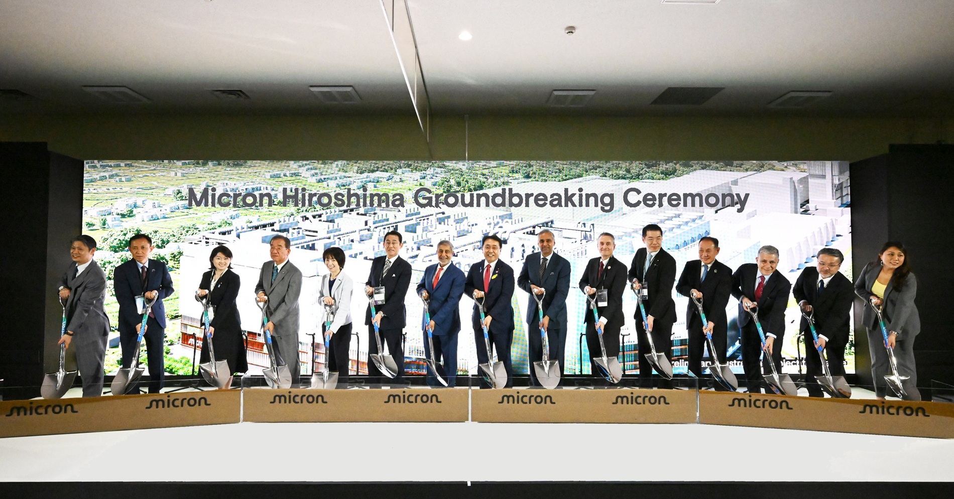
Micron invests 1.5 trillion yen to expand Hiroshima AI facility
💡Major infrastructure investment by Micron highlights the critical supply bottleneck for AI-grade memory.
⚡ 30-Second TL;DR
What Changed
Micron is investing 1.5 trillion yen into its Hiroshima manufacturing site.
Why It Matters
This significant capital expenditure signals a long-term commitment to securing the memory supply chain necessary for high-performance AI hardware.
What To Do Next
Monitor Micron's HBM (High Bandwidth Memory) production roadmap to adjust your hardware procurement strategy for AI clusters.
Who should care:Enterprise & Security Teams
🧠 Deep Insight
AI-generated analysis for this event.
🔑 Enhanced Key Takeaways
- •The Japanese government has pledged significant subsidies to support this expansion, aligning with national efforts to secure a domestic supply chain for advanced semiconductors.
- •This investment is specifically targeted at accelerating the production of High Bandwidth Memory (HBM), which is critical for training and operating large-scale AI models.
- •Micron's Hiroshima facility serves as the company's primary global hub for DRAM manufacturing and R&D, making it central to their 1-gamma process node transition.
- •The expansion is expected to create thousands of high-skilled jobs in the Chugoku region, bolstering the local semiconductor ecosystem.
- •The project is part of a broader multi-year capital expenditure strategy by Micron to increase its global market share in the AI memory sector against South Korean rivals.
📊 Competitor Analysis▸ Show
| Feature | Micron (Hiroshima) | Samsung Electronics | SK Hynix |
|---|---|---|---|
| Primary AI Focus | HBM3E / HBM4 | HBM3E / HBM4 | HBM3E / HBM4 |
| Manufacturing Hub | Japan (Hiroshima) | South Korea | South Korea |
| Market Strategy | Aggressive capacity expansion | Vertical integration | First-mover advantage in HBM |
🛠️ Technical Deep Dive
- The facility is designed to support the transition to 1-gamma (1γ) node technology, which utilizes Extreme Ultraviolet (EUV) lithography.
- The new cleanroom architecture is optimized for the high-density stacking requirements of HBM4, which involves 12-high and 16-high DRAM die stacks.
- Implementation includes advanced thermal management systems to handle the increased power density associated with next-generation AI memory modules.
- Integration of automated material handling systems (AMHS) to increase wafer throughput and reduce contamination risks during the multi-step HBM fabrication process.
🔮 Future ImplicationsAI analysis grounded in cited sources
Micron will achieve a significant increase in its global HBM market share by 2029.
The massive scale of the Hiroshima expansion directly correlates to the production capacity required to compete with established leaders in the AI memory market.
Japan will solidify its position as a critical node in the global AI hardware supply chain.
Substantial government backing combined with Micron's long-term infrastructure commitment creates a stable, high-tech manufacturing base outside of traditional hubs.
⏳ Timeline
2013-07
Micron completes acquisition of Elpida Memory, establishing the Hiroshima plant as a core asset.
2022-09
Micron announces the 1-beta (1β) DRAM node production at the Hiroshima facility.
2023-05
Micron receives official support from the Japanese government for advanced semiconductor production.
2024-02
Micron begins mass production of HBM3E memory, utilizing the Hiroshima site for initial output.
📰
Weekly AI Recap
Read this week's curated digest of top AI events →
👉Related Updates


AI-curated news aggregator. All content rights belong to original publishers.
Original source: ITmedia AI+ (日本) ↗