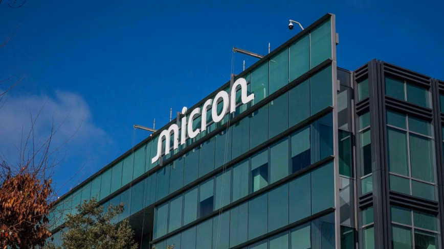
Micron Breaks Ground on $9bn Hiroshima AI Memory Plant
💡Critical infrastructure news: Micron's massive HBM expansion directly impacts the availability of AI compute hardware.
⚡ 30-Second TL;DR
What Changed
Micron invested $9.3 billion in its Hiroshima factory expansion.
Why It Matters
This expansion significantly boosts the supply chain capacity for AI-specific memory, potentially alleviating bottlenecks for high-performance computing hardware.
What To Do Next
Monitor HBM supply availability and lead times when planning your next-generation AI infrastructure or server procurement.
🧠 Deep Insight
AI-generated analysis for this event.
🔑 Enhanced Key Takeaways
- •The Hiroshima expansion is supported by significant subsidies from the Japanese government, which views memory chip production as a critical pillar of national economic security.
- •Micron's Hiroshima facility is the former Elpida Memory plant, which Micron acquired in 2013, marking a decade-plus evolution of the site into a global hub for advanced DRAM.
- •This expansion utilizes EUV (Extreme Ultraviolet) lithography technology, marking the first time Micron has deployed this advanced manufacturing process in Japan.
- •The facility is expected to create hundreds of high-skilled engineering jobs in the Hiroshima prefecture, bolstering local semiconductor ecosystem development.
- •The investment aligns with Micron's broader goal to capture a significant percentage of the HBM market share, aiming to compete directly with South Korean giants Samsung and SK Hynix.
📊 Competitor Analysis▸ Show
| Feature | Micron (Hiroshima) | SK Hynix | Samsung |
|---|---|---|---|
| HBM Focus | HBM3E / HBM4 | HBM3E (Market Leader) | HBM3E / HBM4 |
| Primary Strategy | Capacity Expansion | Aggressive R&D / Partnerships | Vertical Integration |
| Manufacturing | EUV-based DRAM | MR-MUF Packaging | TC-NCF / Hybrid Bonding |
🛠️ Technical Deep Dive
- Focus on HBM3E and next-generation HBM4 architectures utilizing 1-gamma (1γ) process node technology.
- Implementation of Through-Silicon Via (TSV) technology to enable high-density vertical stacking of DRAM dies.
- Integration of EUV lithography to improve pattern fidelity and reduce the number of masks required for advanced DRAM nodes.
- Enhanced thermal management designs to support the high power density requirements of AI accelerators and GPUs.
🔮 Future ImplicationsAI analysis grounded in cited sources
⏳ Timeline
📰 Event Coverage
Weekly AI Recap
Read this week's curated digest of top AI events →
👉Related Updates
Same topic
Explore #semiconductor
Same product
More on high-bandwidth-memory-(hbm)
Same source
Latest from The Next Web (TNW)
India’s CG Semi Launches Production with 200 Million Chips

Peking University Develops Neuromorphic Chip Outperforming Nvidia GPUs
AI Demand Triggers Semiconductor Shortage and Price Hikes
State Post Bureau outlines future of logistics industry
AI-curated news aggregator. All content rights belong to original publishers.
Original source: The Next Web (TNW) ↗