Keysight Advances AI-Designed Semiconductor EDA
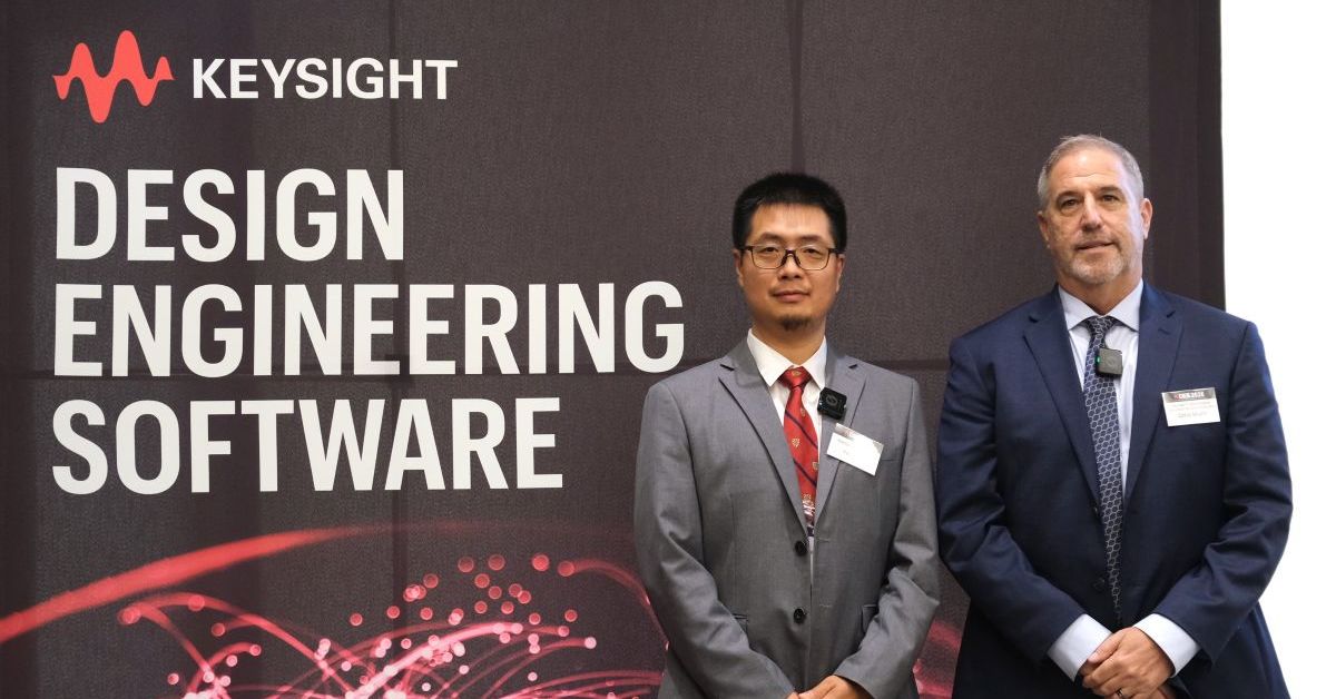
💡See how AI could shift chip design from manual execution toward supervised engineering workflows.
⚡ 30-Second TL;DR
What Changed
Keysight is pursuing EDA workflows in which AI performs more of the semiconductor design work.
Why It Matters
AI-assisted EDA could shorten semiconductor development cycles and help engineers explore more design alternatives. However, human validation remains essential because chip designs must satisfy strict electrical, physical, and manufacturing constraints.
What To Do Next
Map one current chip-design workflow to Keysight's AI-enabled EDA, photonic-design, and multiphysics capabilities, then identify which steps still require human validation.
Key Points
- •Keysight is pursuing EDA workflows in which AI performs more of the semiconductor design work.
- •The company is also developing capabilities for photonic semiconductor design.
- •Multiphysics simulation is part of the next-generation design approach.
- •Human engineers are expected to supervise and validate AI-generated designs.
Weekly AI Recap
Read this week's curated digest of top AI events →
👉Related Updates
AI-curated news aggregator. All content rights belong to original publishers.
Original source: ITmedia AI+ (日本) ↗
This is a summary, not the original. Read the source, or get the weekly briefing.
Weekly AI briefing
One email a week. Unsubscribe anytime.