📊Bloomberg Technology•Freshcollected in 2h
JPMorgan Highlights AI Memory Chip Investment Opportunities
💡Gain insights into the memory chip supply chain bottlenecks affecting AI development and scaling.
⚡ 30-Second TL;DR
What Changed
Memory chip stocks like Micron have seen up to 1,000% gains
Why It Matters
Understanding supply chain constraints is crucial for AI practitioners planning large-scale model training or deployment.
What To Do Next
Analyze HBM availability and lead times when planning hardware procurement for large-scale AI infrastructure projects.
Who should care:Founders & Product Leaders
🧠 Deep Insight
AI-generated analysis for this event.
🔑 Enhanced Key Takeaways
- •High-Bandwidth Memory (HBM3E and HBM4) has become the primary bottleneck for AI server production, forcing manufacturers to prioritize high-margin AI orders over consumer electronics memory.
- •JPMorgan's analysis highlights a shift in capital expenditure from general-purpose cloud infrastructure toward specialized AI-optimized data centers, altering traditional semiconductor cyclicality.
- •The integration of Compute Express Link (CXL) technology is being cited as a critical factor for future memory scaling, allowing for memory pooling that reduces the total cost of ownership for AI clusters.
- •Micron and its peers are increasingly utilizing 'CoWoS' (Chip-on-Wafer-on-Substrate) packaging capacity constraints as a proxy for measuring the ceiling of short-term AI hardware growth.
- •Investment strategies are pivoting toward 'AI-adjacent' sectors, specifically power management integrated circuits (PMICs) and liquid cooling solutions, which are essential to support the thermal demands of high-density memory chips.
📊 Competitor Analysis▸ Show
| Feature | Micron (HBM3E) | SK Hynix (HBM3E) | Samsung (HBM3E) |
|---|---|---|---|
| Market Position | Aggressive Capacity Expansion | Market Leader (NVIDIA Supplier) | Turnaround Strategy |
| Process Node | 1-beta | 10nm-class (5th Gen) | 12nm-class |
| Key Advantage | Power Efficiency | Yield/Volume Leadership | Vertical Integration |
🛠️ Technical Deep Dive
- HBM3E Architecture: Utilizes 8-high or 12-high stacks of DRAM dies connected via Through-Silicon Vias (TSVs) to achieve bandwidths exceeding 1.2 TB/s per stack.
- Thermal Management: Implementation of advanced thermal compression bonding (TCB) to manage heat dissipation in high-density 3D-stacked memory configurations.
- CXL 3.0 Integration: Enables memory expansion and pooling, allowing AI accelerators to access larger memory pools beyond the local HBM capacity, reducing latency for large language model (LLM) inference.
- Die Thinning: Advanced wafer thinning processes are required to stack 12+ layers of DRAM while maintaining standard JEDEC height specifications for server modules.
🔮 Future ImplicationsAI analysis grounded in cited sources
HBM4 will trigger a transition to custom-logic base dies.
The shift to 2048-bit wide interfaces in HBM4 requires memory manufacturers to integrate custom logic directly into the base die, blurring the line between memory and processor design.
Memory manufacturers will experience margin compression by 2027.
As current supply chain bottlenecks ease due to massive capacity expansion, the industry is likely to face a supply glut similar to previous semiconductor cycles.
⏳ Timeline
2023-07
Micron announces sampling of HBM3 Gen2 to address AI demand.
2024-02
Micron begins mass production of HBM3E for NVIDIA's H200 GPUs.
2025-05
Micron reports record revenue growth driven by AI-specific memory demand.
2026-03
Micron announces expansion of advanced packaging facilities to alleviate HBM supply constraints.
📰
Weekly AI Recap
Read this week's curated digest of top AI events →
👉Related Updates
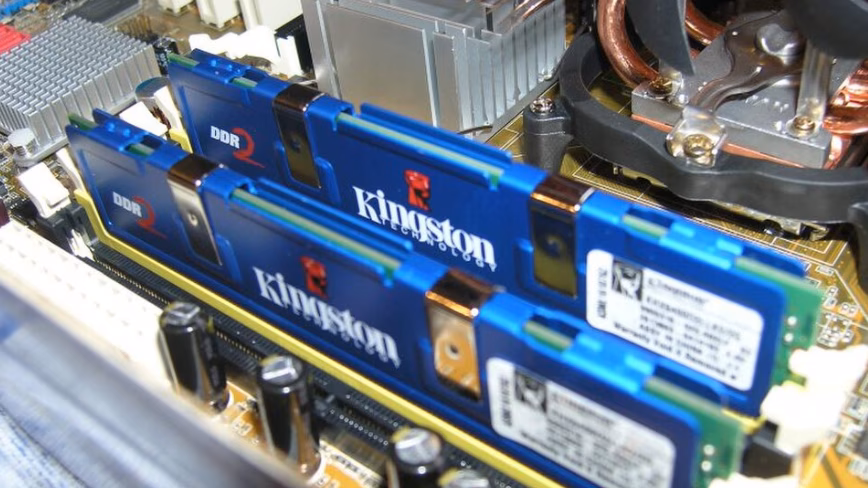
AI Memory Crisis Drives 60% DDR2 Price Hike
The Next Web (TNW)•Jun 22

The trillion-dollar AI hallucination and infrastructure crisis
Computerworld•Jun 22
📊
New Apple CEO Ternus Must Restore Design Focus
Bloomberg Technology•Jun 22
📊
AI Infrastructure Spending Set to Accelerate Further
Bloomberg Technology•Jun 22
AI-curated news aggregator. All content rights belong to original publishers.
Original source: Bloomberg Technology ↗