JCET Eyes Trillion Cap Amid AI Chip Boom
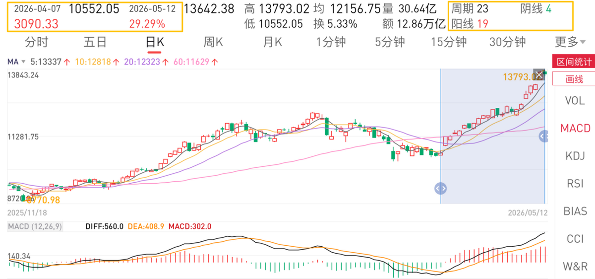
💡10B investment cements JCET's role in AI chip supply chain amid shortages
⚡ 30-Second TL;DR
What Changed
晶片與算力短缺推動長電科技市值穩千億
Why It Matters
Reinforces AI infrastructure bottlenecks, boosting semiconductor packaging firms. AI practitioners should monitor supply chain shifts for compute hardware planning.
What To Do Next
Evaluate JCET's packaging services for your next AI accelerator deployment amid shortages.
Key Points
- •晶片與算力短缺推動長電科技市值穩千億
- •固投 100 億人民幣布局 AI 大週期
- •封測龍頭受益 AI 基礎設施需求爆發
🧠 Deep Insight
AI-generated analysis for this event — not the original article.
🔑 Enhanced Key Takeaways
- •JCET has strategically pivoted toward high-end packaging technologies, specifically 2.5D/3D chiplet integration, to capture demand from high-performance computing (HPC) and AI accelerator manufacturers.
- •The 10 billion yuan investment is heavily focused on expanding capacity at its advanced packaging facilities in Wuxi and Jiangyin to support high-bandwidth memory (HBM) integration and heterogeneous chiplet assembly.
- •The company has recently strengthened its partnership with major domestic Chinese GPU and AI chip designers, positioning itself as a critical alternative to international OSAT (Outsourced Semiconductor Assembly and Test) providers amid ongoing geopolitical supply chain restrictions.
📊 Competitor Analysis▸ Show
| Feature | JCET Group | ASE Technology | Amkor Technology |
|---|---|---|---|
| Core Focus | Advanced Packaging/Chiplets | Full OSAT/System-in-Package | Automotive/Advanced Packaging |
| AI Strategy | Domestic AI Infrastructure | Global AI/HPC Ecosystem | High-Reliability AI/Auto |
| Market Position | Leading Chinese OSAT | Global Market Leader | Tier-1 Global OSAT |
🛠️ Technical Deep Dive
- XDFOI™ Technology Platform: JCET's proprietary high-density packaging solution designed for 2.5D/3D chiplet integration, supporting high-bandwidth, low-latency interconnects.
- Chiplet Integration: Capabilities for multi-die integration on organic substrates, essential for scaling AI compute performance without increasing die size.
- HBM Support: Development of advanced thermal management and fine-pitch micro-bump technology required for integrating High Bandwidth Memory with AI processors.
- Fan-Out Packaging: Expansion of high-density fan-out (FOWLP) capabilities to reduce package thickness and improve electrical performance for mobile and edge AI devices.
🔮 Future ImplicationsAI analysis grounded in cited sources
⏳ Timeline
Weekly AI Recap
Read this week's curated digest of top AI events →
👉Related Updates


AI-curated news aggregator. All content rights belong to original publishers.
Original source: 钛媒体 ↗
This is a summary, not the original. Read the source, or get the weekly briefing.
Weekly AI briefing
One email a week. Unsubscribe anytime.