Intel Processes One Million High-NA EUV Wafers
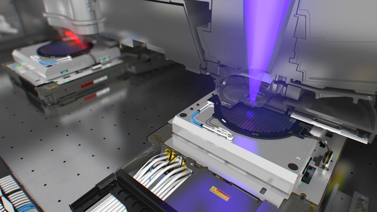
💡Intel’s High-NA EUV milestone could affect the future supply and cost of AI chips.
⚡ 30-Second TL;DR
What Changed
Intel has processed one million wafers with High-NA EUV tools.
Why It Matters
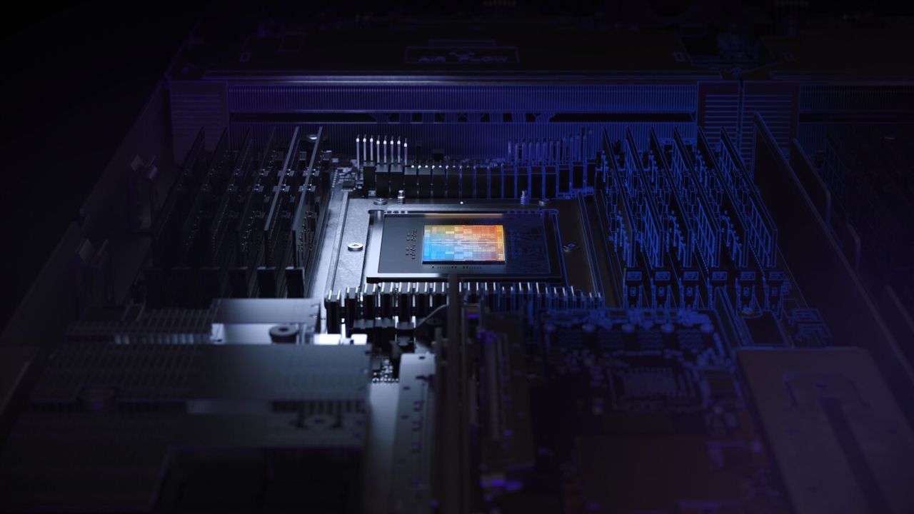
Greater High-NA EUV maturity could improve the long-term supply and economics of advanced chips used in AI accelerators and data-center processors. For AI infrastructure planners, the milestone is a signal about Intel’s foundry readiness, but it does not by itself establish production yield or commercial availability for a specific chip.
What To Do Next
Add Intel Foundry’s High-NA EUV process milestones and 6×12 photomask readiness to your AI accelerator supply-risk checklist, and request validated yield and delivery timelines before committing designs.
Key Points
- •Intel has processed one million wafers with High-NA EUV tools.
- •The company claims its High-NA EUV fleet and process maturity exceed the rest of the industry combined.
- •Intel is developing 6×12 photomasks for larger-area exposure and manufacturing efficiency.
- •The effort targets faster production and lower semiconductor fabrication costs.
Weekly AI Recap
Read this week's curated digest of top AI events →
👉Related Updates
AI-curated news aggregator. All content rights belong to original publishers.
Original source: Tom's Hardware ↗
This is a summary, not the original. Read the source, or get the weekly briefing.
Weekly AI briefing
One email a week. Unsubscribe anytime.