Intel Joins Musk's Terafab AI Chip Project
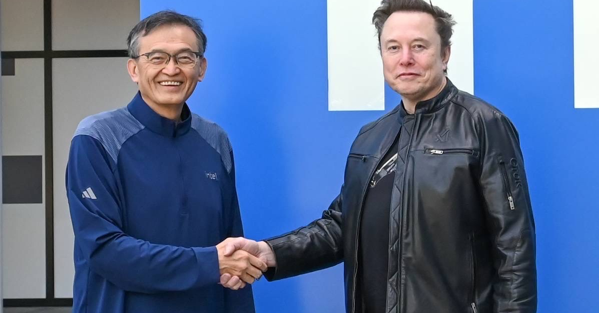
Intel powers Musk's custom AI chip fab for xAI/Tesla—huge for AI infra.
30-Second TL;DR
What Changed
Intel partners on Elon Musk's Terafab initiative
Why It Matters
Accelerates custom AI hardware for Musk ecosystem, reducing external fab dependency. Signals shift in AI infrastructure toward integrated design-manufacturing.
What To Do Next
Track Intel Foundry announcements for Terafab chip access opportunities.
Key Points
- •Intel partners on Elon Musk's Terafab initiative
- •Focuses on AI/robotics chips for Tesla, SpaceX, xAI
- •Provides chip design and manufacturing expertise
- •Enables large-scale production of next-gen chips
Deep Insight
Background and context from public sources — not the original article. 9 sources cited.
Enhanced Key Takeaways
- •Intel's involvement centers on leveraging its 18A process node and advanced packaging capabilities to provide the manufacturing foundation for Terafab, effectively acting as the foundry partner rather than Tesla building a fab from scratch.
- •The Terafab project, valued at $20–25 billion, aims for an ambitious output of 1 terawatt (TW) of annual compute capacity, which is intended to support Tesla's FSD systems, Optimus robots, and SpaceX/xAI orbital AI infrastructure.
- •The partnership aligns with Intel's foundry turnaround strategy and U.S. domestic semiconductor sovereignty goals, positioning Intel as a critical supplier for Musk's ecosystem to mitigate risks associated with reliance on external foundries like TSMC and Samsung.
Competitor Analysis
- Intel (Terafab Partner)
- 18A Process & Advanced Packaging
- TSMC
- Leading-edge Logic (N2/N3)
- Samsung Foundry
- Memory & Logic Integration
- Intel (Terafab Partner)
- High (Domestic Fab focus)
- TSMC
- Moderate (Expanding AZ)
- Samsung Foundry
- Moderate (Expanding TX)
- Intel (Terafab Partner)
- Captive/Dedicated Foundry
- TSMC
- Merchant Foundry
- Samsung Foundry
- Merchant Foundry
| Feature | Intel (Terafab Partner) | TSMC | Samsung Foundry |
|---|---|---|---|
| Primary Focus | 18A Process & Advanced Packaging | Leading-edge Logic (N2/N3) | Memory & Logic Integration |
| U.S. Presence | High (Domestic Fab focus) | Moderate (Expanding AZ) | Moderate (Expanding TX) |
| Strategic Role | Captive/Dedicated Foundry | Merchant Foundry | Merchant Foundry |
Technical Deep Dive
- Process Node: Targeting 2-nanometer class technology (Intel 18A).
- Integration: Vertical integration of logic, memory, and advanced packaging under one roof.
- Output Goal: 1 terawatt (TW) of annual compute capacity.
- Target Scale: Initial output of 100,000 wafer starts per month, with a long-term goal of 1 million wafer starts per month.
- Applications: Edge-inference processors for FSD/Robotaxi/Optimus and radiation-hardened chips for space-based AI data centers.
Future ImplicationsAI analysis grounded in cited sources
Timeline
- 2025-11Musk publicly discusses potential for Intel-Tesla collaboration on AI5 chips.
- 2026-03Elon Musk officially unveils the $20-25 billion Terafab project in Austin, Texas.
- 2026-04Intel officially joins the Terafab project as a key manufacturing and design partner.
Sources (9)
Factual claims are grounded in the sources below. Forward-looking analysis is AI-generated interpretation.
Weekly AI Recap
Read this week's curated digest of top AI events →
Related Updates
AI-curated news aggregator. All content rights belong to original publishers.
Original source: ITmedia AI+ (日本) ↗
This is a summary, not the original. Read the source, or get the weekly briefing.
The weekly digest
One email a week. Unsubscribe anytime.