Intel Hits One Million High-NA EUV Wafers
💡Intel’s EUV manufacturing lead could reshape the supply outlook for next-generation AI chips.
⚡ 30-Second TL;DR
What Changed
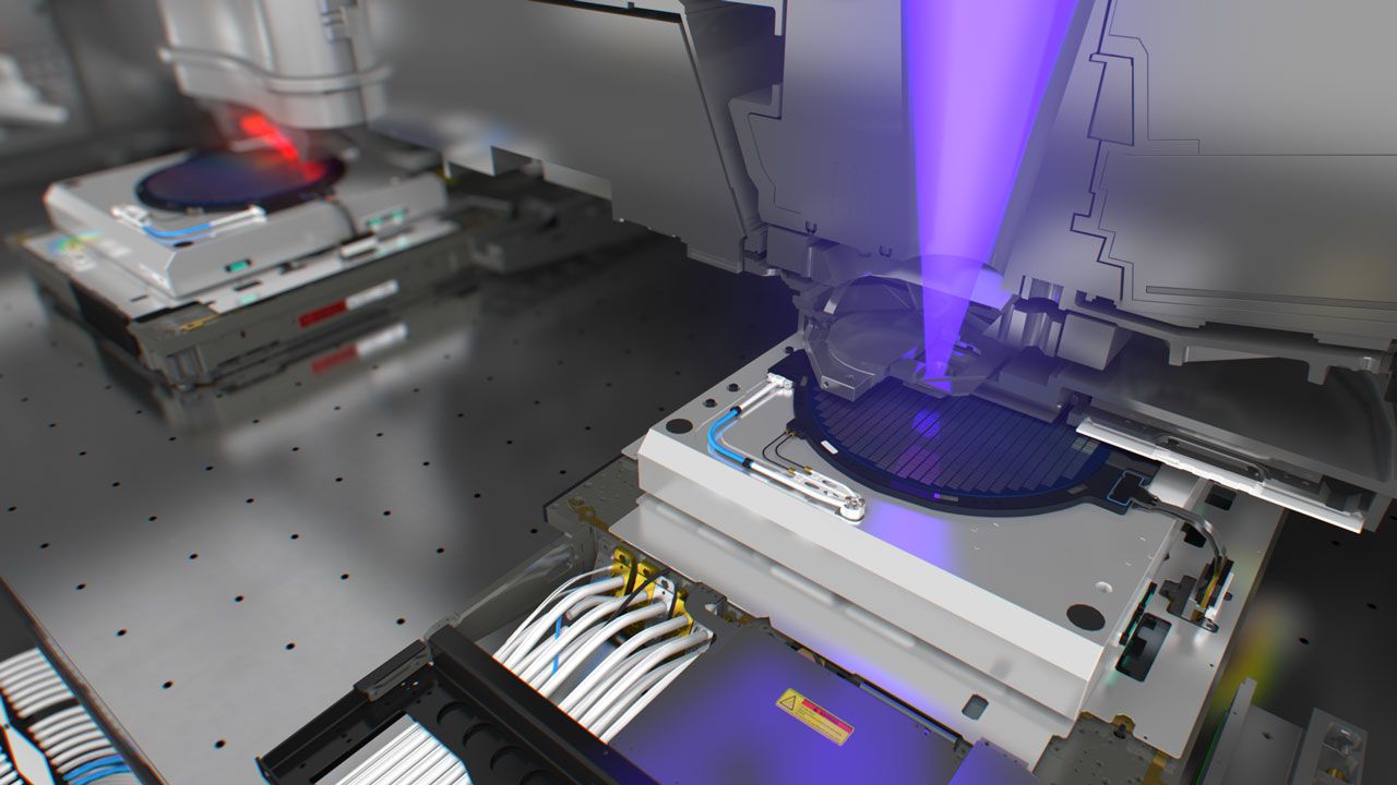
Intel has processed over one million wafers with High-NA EUV equipment.
Why It Matters
Greater High-NA EUV process maturity could help Intel compete for advanced AI-chip and leading-edge foundry workloads. If the larger photomask approach scales successfully, it may improve wafer economics and shorten manufacturing cycles.
What To Do Next
Review Intel Foundry’s High-NA EUV and advanced-packaging roadmap before committing future AI-chip designs to a single manufacturing partner.
Key Points
- •Intel has processed over one million wafers with High-NA EUV equipment.
- •The milestone reportedly exceeds the combined High-NA EUV wafer volume of the rest of the industry.
- •Intel is developing 6×12 photomasks to improve throughput and lower production costs.
Weekly AI Recap
Read this week's curated digest of top AI events →
👉Related Updates

AI-curated news aggregator. All content rights belong to original publishers.
Original source: Tom's Hardware ↗
This is a summary, not the original. Read the source, or get the weekly briefing.
Weekly AI briefing
One email a week. Unsubscribe anytime.