Intel Foundry Nears Big Orders from Apple, AMD, Google, Nvidia
💡Intel + Nvidia/Google foundry shift reshapes AI chip supply
⚡ 30-Second TL;DR
What Changed
Intel Foundry poised for contracts from Apple, AMD, Google, Nvidia.
Why It Matters
Could establish Intel as TSMC rival for AI chips, diversifying supply chains for Nvidia/Google AI hardware and stabilizing costs amid shortages.
What To Do Next
Access Intel 14A PDK via their portal to prototype AI accelerator designs.
Key Points
- •Intel Foundry poised for contracts from Apple, AMD, Google, Nvidia.
- •UBS: Intel on 'the last kick' for multiple major deals.
- •14A process 1.0 PDK release accelerates client decisions.
- •Announcements expected this autumn.
🧠 Deep Insight
AI-generated analysis for this event — not the original article.
🔑 Enhanced Key Takeaways
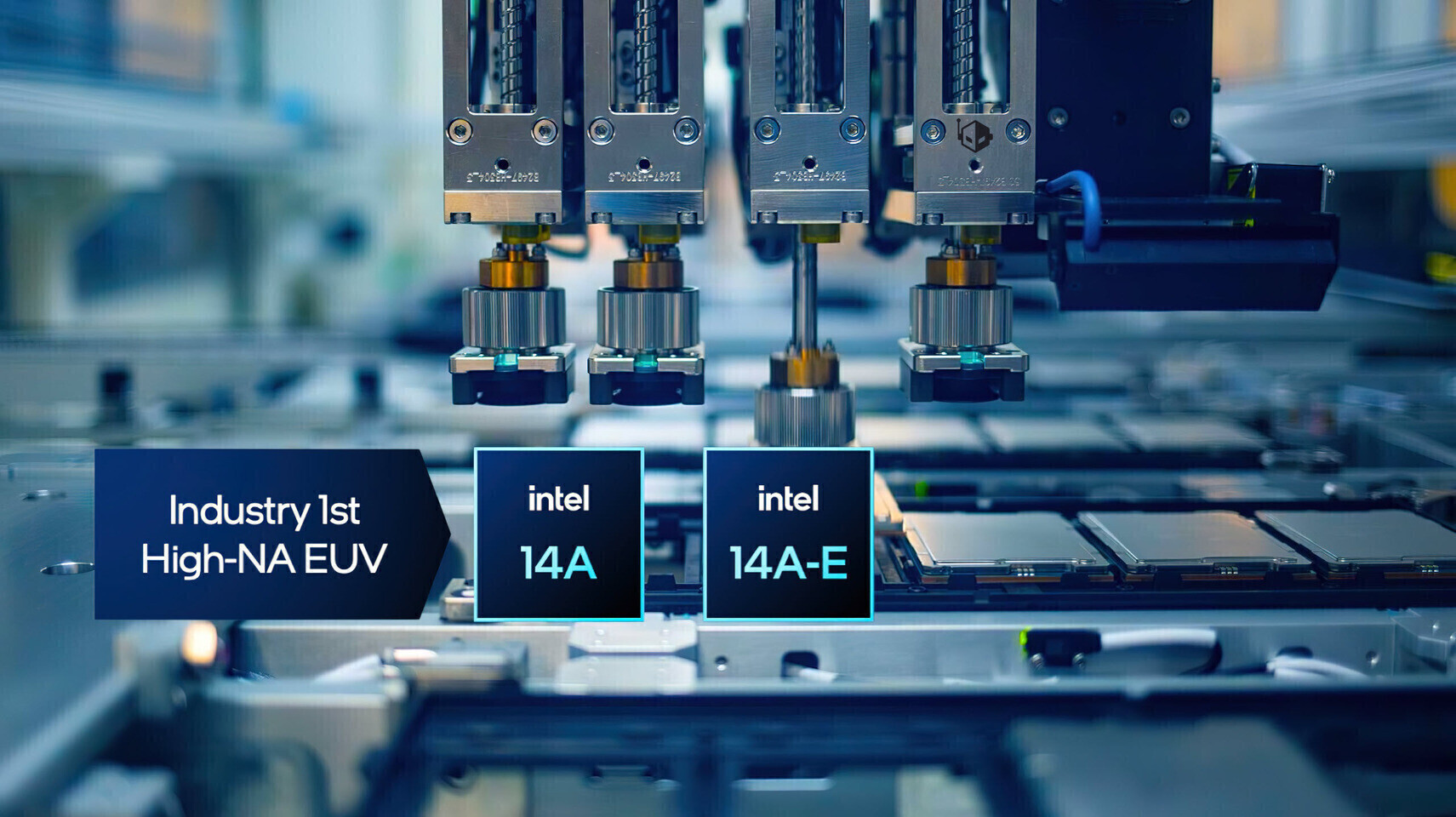
- •The 14A process node represents Intel's transition to High-NA EUV lithography, which is critical for achieving the density and power efficiency required by hyperscalers and AI chip designers.
- •Intel Foundry's strategy involves a 'systems foundry' approach, offering advanced packaging (Foveros) and chiplet interconnects (UCIe) alongside wafer fabrication to attract fabless companies.
- •The potential deals are contingent on Intel demonstrating yield maturity on the 14A node, as major clients like Apple and Nvidia have historically prioritized TSMC due to its proven high-volume manufacturing reliability.
📊 Competitor Analysis▸ Show
| Feature | Intel Foundry (14A) | TSMC (N2/A16) | Samsung Foundry (SF2/SF1.4) |
|---|---|---|---|
| Lithography | High-NA EUV | EUV / High-NA EUV | EUV / High-NA EUV |
| Packaging | Foveros / EMIB | CoWoS / SoIC | I-Cube / X-Cube |
| Market Position | Challenger / Turnaround | Dominant / Incumbent | Secondary / Alternative |
🛠️ Technical Deep Dive
- •14A Node: Utilizes High-NA (0.55 numerical aperture) EUV lithography to reduce multi-patterning complexity and improve feature resolution.
- •Power Delivery: Incorporates backside power delivery (PowerVia) to decouple power and signal routing, significantly reducing IR drop and improving transistor density.
- •Transistor Architecture: Employs RibbonFET (Gate-All-Around) technology to provide superior electrostatic control compared to traditional FinFET designs.
- •Ecosystem: Supports the Universal Chiplet Interconnect Express (UCIe) standard, enabling heterogeneous integration of chiplets from different vendors.
🔮 Future ImplicationsAI analysis grounded in cited sources
⏳ Timeline
Weekly AI Recap
Read this week's curated digest of top AI events →
👉Related Updates
AI-curated news aggregator. All content rights belong to original publishers.
Original source: cnBeta (Full RSS) ↗
This is a summary, not the original. Read the source, or get the weekly briefing.
The weekly digest
One email a week. Unsubscribe anytime.