Intel 18A-P Delivers 30% More Low-Voltage Frequency
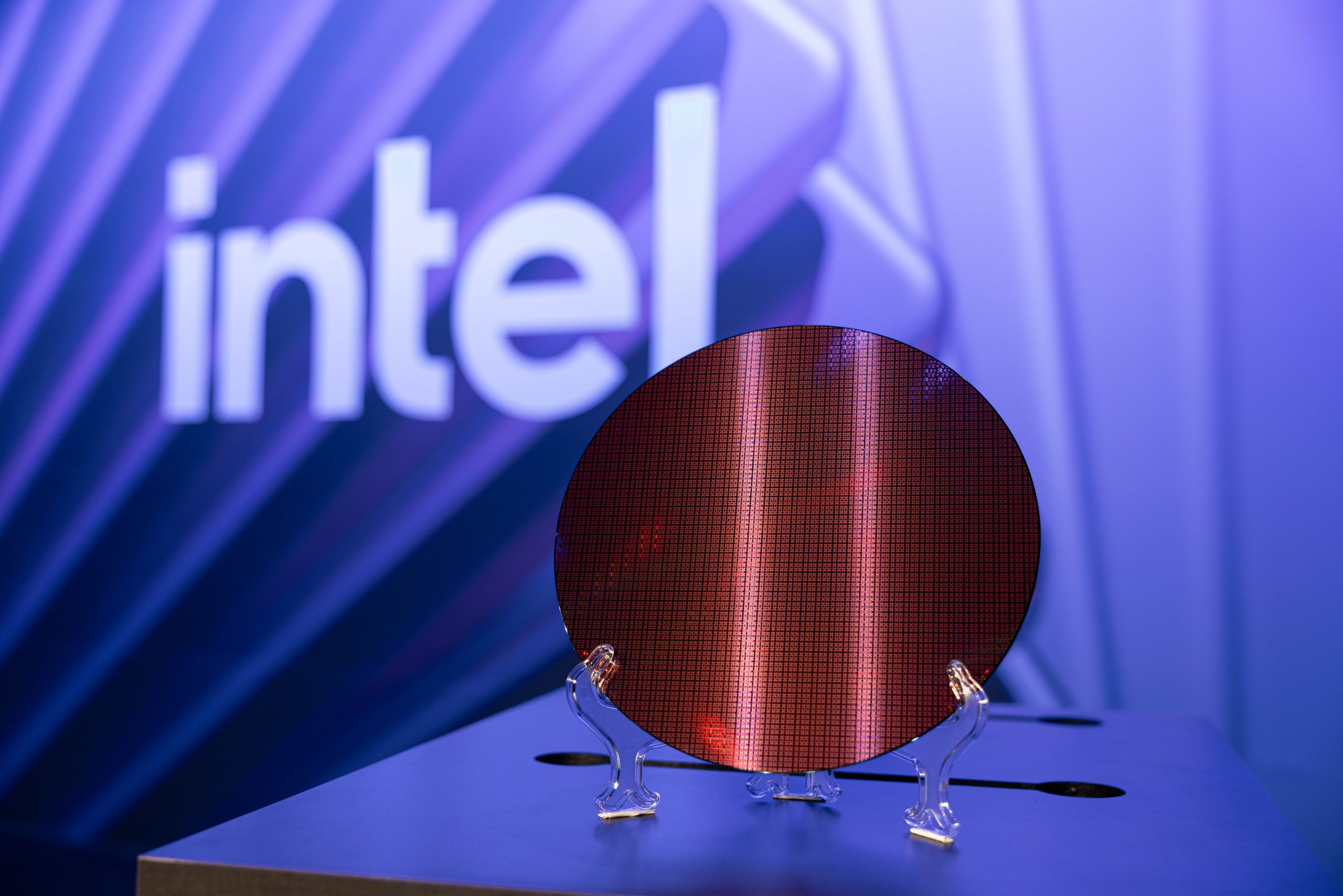
💡A potentially meaningful low-voltage efficiency gain for future AI and data-center processors.
⚡ 30-Second TL;DR
What Changed
The reported measurement was taken at a low operating voltage of 0.5V.
Why It Matters
Higher frequency at low voltage could improve performance-per-watt for AI accelerators, CPUs, and edge inference systems built on x86 platforms. If these results scale across products, they may strengthen Intel’s position in power-constrained compute markets.
What To Do Next
Track Intel’s 18A-P product disclosures and compare measured performance-per-watt data before selecting future x86 servers for AI inference workloads.
Key Points
- •The reported measurement was taken at a low operating voltage of 0.5V.
- •Intel claims up to a 30% frequency improvement for x86 production silicon.
- •18A-P combines GAA transistors with backside power delivery.
- •The process also adds Power Boost technology and more metal layers.
🧠 Deep Insight
Background and context from public sources — not the original article. 9 sources cited.
🔑 Enhanced Key Takeaways
- •Intel 18A-P provides a 9% performance gain at iso-power or an 18% power reduction at iso-performance compared to the base 18A node.
- •The process utilizes a dual-contact architecture known as Power Boost, which employs ultra-low-resistance contacts on both sides of the silicon to increase drive current.
- •Technical refinements in 18A-P result in a 20–40% improvement in thermal resistance and a 10–30% reduction in via resistance.
- •The process maintains full design-rule compatibility with the base 18A node, allowing for seamless migration without requiring complete layout or library redesigns.
- •Intel has confirmed that 18A-P has reached the risk production milestone as of August 2026, with the Diamond Rapids Xeon 7 processors identified as the primary launch vehicle.
📊 Competitor Analysis▸ Show
| Feature | Intel 18A-P | TSMC N2 (2nm) | Samsung 2nm (SF2) |
|---|---|---|---|
| Transistor Architecture | RibbonFET (GAA) | NanoFlex (GAA) | MBCFET (GAA) |
| Power Delivery | PowerVia (Backside) | Backside Power Rail | Backside Power Delivery |
| Status (Aug 2026) | Risk Production | High-Volume Production | Risk Production |
🛠️ Technical Deep Dive
- RibbonFET: Gate-All-Around (GAA) transistor architecture providing superior electrostatic control.
- PowerVia: Backside power delivery network that decouples power and signal routing to reduce IR drop.
- Power Boost: Dual-contact architecture utilizing front and back ultra-low-resistance contacts to maximize drive current.
- Thermal/Resistance: 20-40% reduction in thermal resistance and 10-30% reduction in via resistance compared to 18A.
- Design Compatibility: Full design-rule parity with 18A to facilitate rapid customer adoption.
🔮 Future ImplicationsAI analysis grounded in cited sources
⏳ Timeline
📎 Sources (9)
Factual claims are grounded in the sources below. Forward-looking analysis is AI-generated interpretation.
Weekly AI Recap
Read this week's curated digest of top AI events →
👉Related Updates
AI-curated news aggregator. All content rights belong to original publishers.
Original source: cnBeta (Full RSS) ↗
This is a summary, not the original. Read the source, or get the weekly briefing.
Weekly AI briefing
One email a week. Unsubscribe anytime.