India Opens $13.4B Chip Subsidy Fund
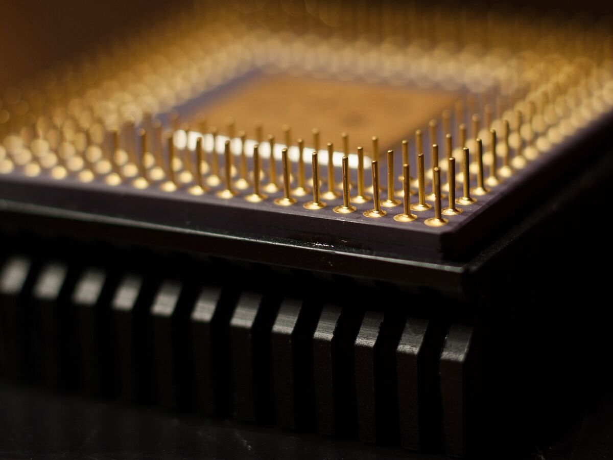
💡India’s new subsidies could reshape where AI chips are designed and built.
⚡ 30-Second TL;DR
What Changed
India has set aside $13.4 billion for semiconductor-related support.
Why It Matters
Lowering the cost of chip design and equipment could attract startups, global manufacturers, and AI infrastructure investments to India. It may also diversify AI hardware supply chains beyond established semiconductor hubs.
What To Do Next
Review India’s semiconductor fund guidelines and assess whether your AI hardware, chip-design, or infrastructure roadmap qualifies for support.
Key Points
- •India has set aside $13.4 billion for semiconductor-related support.
- •The program covers chip design and semiconductor equipment.
- •The subsidies could help develop local AI chip and hardware capabilities.
🧠 Deep Insight
Background and context from public sources — not the original article. 7 sources cited.
🔑 Enhanced Key Takeaways
- •The initiative, branded as 'Semicon 2.0', expands the total fiscal outlay to ₹1,27,500 crore, significantly increasing the scope from the initial ₹76,000 crore allocated under ISM 1.0.
- •The program is structured around a six-pillar strategy that includes wafer fabrication, ATMP/OSAT, equipment manufacturing, chip design, R&D, and talent development.
- •Incentives include a 30% capital subsidy and a five-year production-linked incentive (PLI) specifically targeting semiconductor materials and equipment manufacturers.
- •The policy introduces targeted support for Indian-owned startups and MSMEs, including seed funding, equity co-investment, and royalty financing to foster indigenous intellectual property.
- •As of March 2026, the preceding phase had already secured investment commitments totaling ₹1.6 trillion, resulting in the approval of 10 semiconductor units including 2 fabrication plants.
📊 Competitor Analysis▸ Show
| Feature | India (Semicon 2.0) | USA (CHIPS Act) | EU (Chips Act) |
|---|---|---|---|
| Primary Focus | Design, Equipment, ATMP | Advanced Logic/Memory Fabs | Advanced Fabs & R&D |
| Incentive Model | 30% CapEx + PLI | 25% Investment Tax Credit | Grants & State Aid Flexibility |
| Target Market | Startups, MSMEs, Global Supply | Domestic Manufacturing Security | Sovereignty & Supply Resilience |
🛠️ Technical Deep Dive
- Focuses on the full semiconductor value chain including front-end wafer fabrication and back-end assembly, testing, marking, and packaging (ATMP).
- Supports the development of indigenous IP through royalty financing and equity co-investment for domestic design firms.
- Emphasizes the localization of semiconductor equipment manufacturing to reduce reliance on imported capital goods.
- Integrates research and development mandates to bridge the gap between academic training and industrial fabrication requirements.
🔮 Future ImplicationsAI analysis grounded in cited sources
⏳ Timeline
📎 Sources (7)
Factual claims are grounded in the sources below. Forward-looking analysis is AI-generated interpretation.
Weekly AI Recap
Read this week's curated digest of top AI events →
👉Related Updates


AI-curated news aggregator. All content rights belong to original publishers.
Original source: Bloomberg Technology ↗
This is a summary, not the original. Read the source, or get the weekly briefing.
Weekly AI briefing
One email a week. Unsubscribe anytime.