Hwatsing Unveils Six-Inch Wafer Metrology System
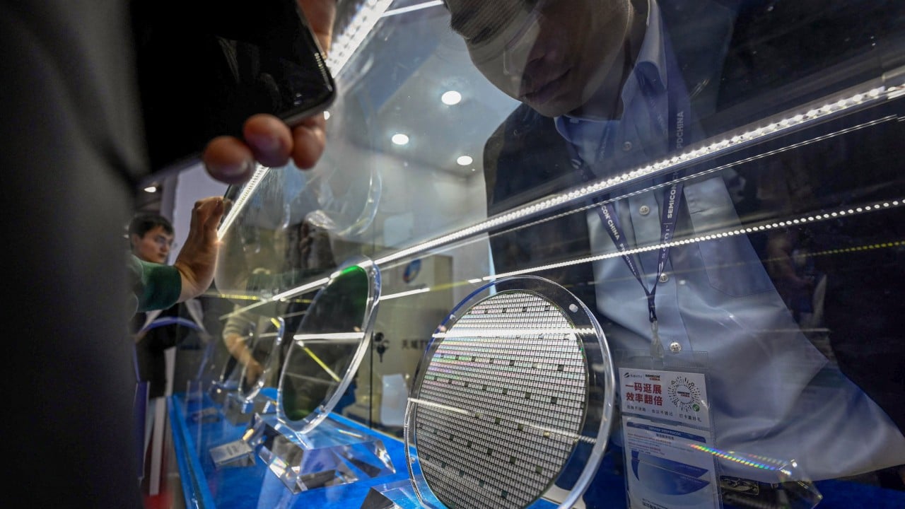
China’s wafer-polishing tool gains could reshape the supply chain behind future AI chips.
30-Second TL;DR
What Changed
Hwatsing Technology announced a new metrology system designed for six-inch wafers.
Why It Matters
Improved domestic polishing and measurement equipment could strengthen China’s semiconductor supply chain and indirectly support local AI-chip production. However, the announcement does not indicate independence from foreign suppliers in leading-edge fabrication.
What To Do Next
Assess whether your AI-chip supply-chain roadmap depends on imported polishing and metrology equipment, and identify qualified domestic alternatives such as Hwatsing Technology.
Key Points
- •Hwatsing Technology announced a new metrology system designed for six-inch wafers.
- •The system targets ultra-precise measurement in the chemical mechanical polishing workflow.
- •The announcement reflects China’s progress in chip-manufacturing tools beyond lithography.
- •China’s semiconductor industry remains dependent on foreign suppliers for more complex manufacturing procedures.
Deep Insight
AI-generated analysis for this event — not the original article.
Enhanced Key Takeaways
- •Hwatsing Technology, formally known as Tianjin Hwatsing Technology, is primarily recognized as China's dominant supplier of Chemical Mechanical Polishing (CMP) equipment, holding a significant domestic market share.
- •The move into metrology represents a strategic vertical integration, allowing Hwatsing to offer 'process-plus-inspection' solutions that compete with integrated workflows from global leaders like Applied Materials.
- •Six-inch wafer production remains critical for power semiconductors, MEMS, and analog chips, sectors where China is aggressively expanding capacity to achieve supply chain autonomy.
- •Hwatsing's expansion into metrology is supported by China's 'Big Fund' (National Integrated Circuit Industry Investment Fund), which has prioritized domestic equipment localization to mitigate US-led export controls.
- •The new system utilizes advanced optical sensing technology to detect sub-nanometer surface defects, a capability previously dominated by Japanese and American metrology firms.
Competitor Analysis
- Hwatsing (New System)
- CMP-Integrated Metrology
- Applied Materials (Producer)
- Full-Fab Solutions
- KLA Corporation (Metrology)
- Standalone Metrology/Inspection
- Hwatsing (New System)
- 6-inch focus
- Applied Materials (Producer)
- 8-inch / 12-inch focus
- KLA Corporation (Metrology)
- 8-inch / 12-inch focus
- Hwatsing (New System)
- Emerging Domestic
- Applied Materials (Producer)
- Global Leader
- KLA Corporation (Metrology)
- Global Leader
| Feature | Hwatsing (New System) | Applied Materials (Producer) | KLA Corporation (Metrology) |
|---|---|---|---|
| Primary Focus | CMP-Integrated Metrology | Full-Fab Solutions | Standalone Metrology/Inspection |
| Wafer Size Support | 6-inch focus | 8-inch / 12-inch focus | 8-inch / 12-inch focus |
| Market Position | Emerging Domestic | Global Leader | Global Leader |
Technical Deep Dive
- System utilizes multi-wavelength optical interference for surface topography mapping.
- Integration of AI-driven defect classification algorithms to reduce false-positive rates during post-CMP inspection.
- Designed for high-throughput measurement to match the cycle times of Hwatsing's existing CMP polishing platforms.
- Employs non-destructive measurement techniques to ensure wafer integrity for sensitive power device substrates.
Future ImplicationsAI analysis grounded in cited sources
Timeline
- 2013-05Hwatsing Technology is established in Tianjin, China.
- 2018-06Hwatsing achieves mass production of its first-generation CMP equipment for 12-inch wafers.
- 2022-03Hwatsing completes its IPO on the Shanghai Stock Exchange STAR Market.
- 2024-11Hwatsing announces expansion of R&D facilities to focus on advanced packaging and metrology integration.
Weekly AI Recap
Read this week's curated digest of top AI events →
Related Updates



AI-curated news aggregator. All content rights belong to original publishers.
Original source: SCMP Technology ↗
This is a summary, not the original. Read the source, or get the weekly briefing.
The weekly digest
One email a week. Unsubscribe anytime.