Huawei's Logic Folding Breakthrough Boosts 5nm Chip Density
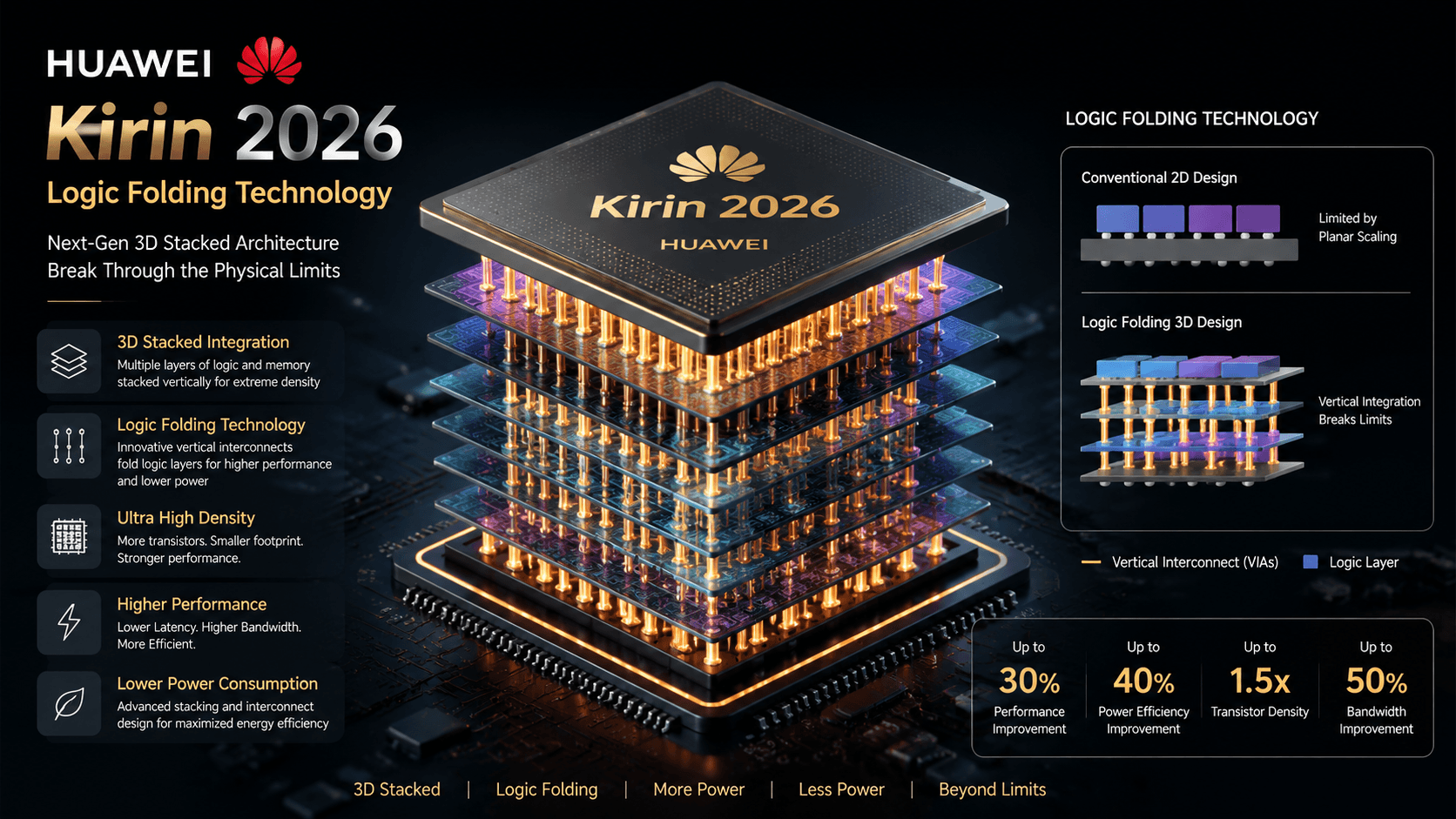
💡A major breakthrough in chip architecture that could redefine AI hardware production without EUV reliance.
⚡ 30-Second TL;DR
What Changed
Introduces Logic Folding technology to optimize transistor layout
Why It Matters
This breakthrough could significantly lower the barrier for high-performance AI hardware production under trade restrictions. It suggests a path for domestic chip manufacturers to remain competitive in AI compute density.
What To Do Next
Monitor the availability of Kirin 2026-based hardware to evaluate its performance-per-watt for edge AI inference tasks.
Key Points
- •Introduces Logic Folding technology to optimize transistor layout
- •Achieves a transistor density of 175MTr/mm² on 5nm nodes
- •Bypasses the need for advanced EUV lithography for performance gains
🧠 Deep Insight
AI-generated analysis for this event — not the original article.
🔑 Enhanced Key Takeaways
- •The 'Tao's Law V2' framework utilizes a proprietary 3D-stacking logic architecture that reconfigures standard cell libraries to reduce footprint by 22% compared to traditional 5nm layouts.
- •Huawei's approach integrates AI-driven placement and routing (PnR) algorithms specifically designed to mitigate the signal integrity issues typically associated with high-density logic folding.
- •This technology is reportedly being deployed in the Kirin 9000 series refresh, allowing Huawei to maintain competitive performance metrics despite ongoing restrictions on accessing sub-7nm EUV equipment.
- •Industry analysts note that Logic Folding shifts the bottleneck from lithography resolution to thermal management, requiring Huawei to implement new micro-fluidic cooling solutions in mobile chipsets.
- •The research paper indicates that Logic Folding is compatible with DUV (Deep Ultraviolet) multi-patterning processes, effectively extending the economic viability of older lithography hardware.
📊 Competitor Analysis▸ Show
| Feature | Huawei (Logic Folding) | TSMC (N5/N4P) | Intel (Intel 4/3) |
|---|---|---|---|
| Lithography | DUV Multi-patterning | EUV | EUV |
| Density (MTr/mm²) | 175 | ~171-180 | ~170-200 |
| Strategy | Architectural Optimization | Process Scaling | Process Scaling |
🛠️ Technical Deep Dive
- Logic Folding utilizes a vertical cell-folding technique that stacks PMOS and NMOS transistors in a non-standard orientation to minimize interconnect length.
- The implementation relies on a custom EDA (Electronic Design Automation) toolchain that bypasses standard commercial libraries to optimize for DUV-specific constraints.
- Thermal dissipation is managed through a modified back-end-of-line (BEOL) metal stack that increases copper thickness in high-density regions.
- The 175MTr/mm² density is achieved by reducing the track height of standard cells from 6T to 5T without compromising drive current.
🔮 Future ImplicationsAI analysis grounded in cited sources
⏳ Timeline
Weekly AI Recap
Read this week's curated digest of top AI events →
👉Related Updates
AI-curated news aggregator. All content rights belong to original publishers.
Original source: Pandaily ↗
This is a summary, not the original. Read the source, or get the weekly briefing.
Weekly AI briefing
One email a week. Unsubscribe anytime.