HEPS Synchrotron Shifts Focus to Industrial Impact
💡Learn how state-of-the-art physics facilities are pivoting to support industrial hardware and semiconductor R&D.
⚡ 30-Second TL;DR
What Changed
HEPS shifts research focus from academic output to industrial utility
Why It Matters
This shift signals a broader trend in Chinese state-funded research to prioritize tangible economic and industrial outcomes over theoretical research, potentially accelerating hardware innovation cycles.
What To Do Next
If you are working on material science or hardware R&D, explore partnership opportunities with HEPS for high-resolution structural analysis of your prototypes.
🧠 Deep Insight
AI-generated analysis for this event.
🔑 Enhanced Key Takeaways
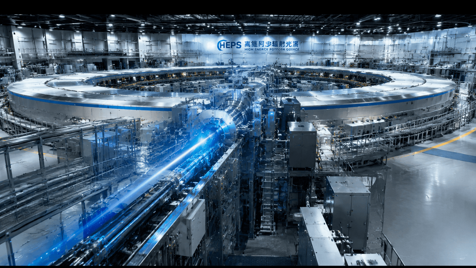
- •HEPS (High Energy Photon Source) is located in Huairou Science City, Beijing, and is a key component of China's national major science and technology infrastructure projects.
- •The facility utilizes a diffraction-limited storage ring (DLSR) design, which significantly increases the brightness and coherence of the X-ray beams compared to third-generation sources.
- •The project is managed by the Institute of High Energy Physics (IHEP) under the Chinese Academy of Sciences (CAS).
- •HEPS achieved its first light in 2024, marking a critical transition from the construction phase to the commissioning and user-operation phase.
- •The facility's beamlines are specifically designed to support in-situ and operando experiments, allowing researchers to observe material changes in real-time under working conditions.
📊 Competitor Analysis▸ Show
| Feature | HEPS (China) | ESRF-EBS (France) | APS-U (USA) |
|---|---|---|---|
| Energy Level | 6.0 GeV | 6.0 GeV | 6.0 GeV |
| Technology | 4th Gen DLSR | 4th Gen DLSR | 4th Gen DLSR |
| Primary Focus | Industrial/Academic | Academic/Industrial | Academic/Industrial |
| Status | Operational | Operational | Operational |
🛠️ Technical Deep Dive
- Energy: 6 GeV storage ring with a circumference of 1,360.4 meters.
- Emittance: Ultra-low horizontal emittance of less than 60 pm·rad.
- Brightness: Peak brightness exceeding 10^22 photons/s/mm^2/mrad^2/0.1%BW.
- Beamlines: Designed to host over 90 beamlines at full capacity, focusing on high-energy, high-flux X-ray imaging and spectroscopy.
- Stability: Sub-micron beam stability achieved through advanced vibration isolation and feedback systems.
🔮 Future ImplicationsAI analysis grounded in cited sources
⏳ Timeline
Weekly AI Recap
Read this week's curated digest of top AI events →
👉Related Updates

Samsung plans 90 trillion won buyback for employee bonuses
TSMC to Raise Prices for 7nm and Below Nodes

Apple Supplier Luxshare Clears Hong Kong Listing Hurdle
Leveraged Korea ETFs Sell $6B in Chip Stocks
AI-curated news aggregator. All content rights belong to original publishers.
Original source: Pandaily ↗