Google Partners with Samsung to Ease AI Chip Shortage
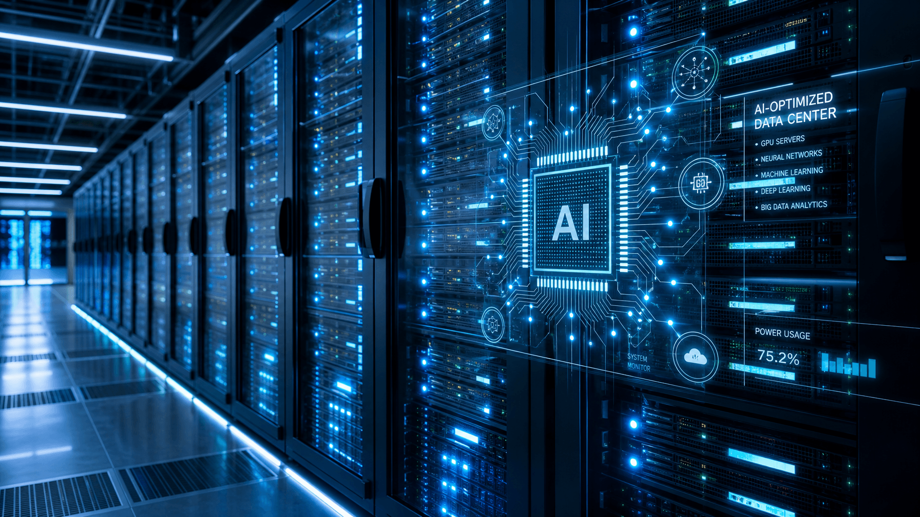
💡Understand how supply chain shifts at Google could impact your future AI compute costs and hardware availability.
⚡ 30-Second TL;DR
What Changed
Google is diversifying its chip manufacturing beyond current partners to Samsung.
Why It Matters
This diversification strategy may stabilize Google's hardware roadmap for TPU production. It signals a broader industry trend where hyperscalers must secure multiple foundry partners to maintain AI development velocity.
What To Do Next
Monitor Google Cloud's TPU availability and hardware announcements to adjust your infrastructure scaling strategy accordingly.
Key Points
- •Google is diversifying its chip manufacturing beyond current partners to Samsung.
- •The AI boom is causing a significant strain on global semiconductor supply chains.
- •Strategic partnerships are becoming essential to secure high-end AI hardware production.
🧠 Deep Insight
Background and context from public sources — not the original article. 31 sources cited.
🔑 Enhanced Key Takeaways
- •Google is implementing a 'split manufacturing strategy' for its upcoming 10th-generation Tensor Processing Unit (TPU), codenamed 'Icefish,' where TSMC will produce the primary compute component using its 1.4-nanometer process, and Samsung will manufacture a separate memory-interface component (I/O die) using its 2-nanometer process.
- •Beyond Samsung, Google has been actively diversifying its AI chip supply chain, collaborating with design partners such as Broadcom, MediaTek, and Marvell for various custom chips, including inference-optimized TPUs and Memory Processing Units (MPUs).
- •The global AI chip shortage extends beyond just processing units to include High Bandwidth Memory (HBM), which is critical for training large AI models, leading to supply constraints and increased prices across the semiconductor industry.
- •Google is also reportedly in talks with Intel to manufacture more than three million TPUs by 2028, further expanding its manufacturing partnerships beyond TSMC and the newly reported Samsung collaboration.
🛠️ Technical Deep Dive
- TPUs are Application-Specific Integrated Circuits (ASICs) developed by Google for neural network machine learning, specifically optimized for matrix multiplication and tensor operations.
- The architecture features TensorCores, each containing one or more Matrix-Multiply Units (MXUs), a vector unit, and a scalar unit. MXUs are systolic arrays, with earlier versions having 128x128 multiply-accumulators and later versions (v6e, v7x) having 256x256.
- TPUs utilize bfloat16 inputs for multiplies and perform accumulations in FP32 format.
- Inter-chip communication is crucial, with TPUs arranged in 3D mesh or 3D torus topologies, scaling up to 9,216 chips in a superpod for the Ironwood (TPU v7) generation, delivering 42.5 FP8 exaflops.
- High Bandwidth Memory (HBM) is a key component, with Ironwood (TPU v7) featuring 192GB of HBM3e memory per chip with 7.2-7.4 TB/s bandwidth.
- The upcoming 10th-generation TPU, 'Icefish,' will reportedly use TSMC's 1.4nm process for the main compute and Samsung's 2nm process for the memory I/O die, leveraging Samsung's expertise in HBM integration and advanced packaging.
- Google's 8th generation TPUs (TPU 8t for training and TPU 8i for inference) represent a bifurcation of architecture, optimized for specific workloads, and are hosted on Google's custom Arm-based Axion CPUs.
🔮 Future ImplicationsAI analysis grounded in cited sources
⏳ Timeline
📎 Sources (31)
Factual claims are grounded in the sources below. Forward-looking analysis is AI-generated interpretation.
- tradingview.com
- investing.com
- spokesman.com
- channelnewsasia.com
- chosun.com
- gate.com
- koreaherald.com
- letsdatascience.com
- moomoo.com
- thenextweb.com
- semicone.com
- forbes.com
- businessinsider.com
- substack.com
- smarterarticles.co.uk
- tomshardware.com
- americanbazaaronline.com
- businesskorea.co.kr
- wikipedia.org
- google.com
- google.com
- uncoveralpha.com
- introl.com
- medium.com
- google.com
- youtube.com
- fool.com
- blog.google
- orhanergun.net
- bytebytego.com
- gurufocus.com
Weekly AI Recap
Read this week's curated digest of top AI events →
👉Related Updates

AI-curated news aggregator. All content rights belong to original publishers.
Original source: Pandaily ↗
This is a summary, not the original. Read the source, or get the weekly briefing.
The weekly digest
One email a week. Unsubscribe anytime.