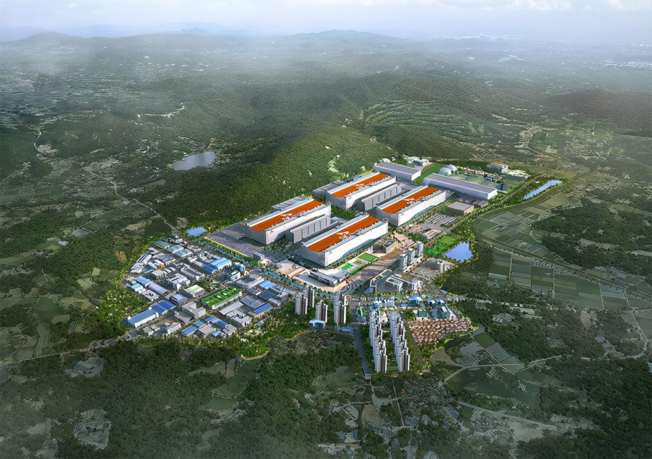
Samsung accelerates Yongin chip fab launch to 2029
💡Faster chip production timelines directly impact the availability and cost of next-gen AI hardware.
⚡ 30-Second TL;DR
What Changed
Samsung's first Yongin fab scheduled for 2029 launch
Why It Matters
The accelerated timeline increases global high-end chip supply capacity, potentially lowering costs for AI hardware developers in the long run.
What To Do Next
Monitor Samsung's foundry roadmap updates to align your hardware procurement strategy for future AI infrastructure projects.
Key Points
- •Samsung's first Yongin fab scheduled for 2029 launch
- •Timeline accelerated by 1-2 years due to government support
- •Yongin site serves as the core base for next-gen semiconductor manufacturing
🧠 Deep Insight
AI-generated analysis for this event — not the original article.
🔑 Enhanced Key Takeaways
- •The Yongin semiconductor cluster is designated as a 'National Industrial Complex,' with the South Korean government committing to expedite power, water, and road infrastructure to overcome previous delays.
- •Samsung's investment in the Yongin cluster is part of a massive 360 trillion won commitment aimed at establishing the world's largest semiconductor mega-cluster by 2047.
- •The accelerated timeline is partially driven by the urgent need to secure advanced node capacity (sub-2nm) to compete with TSMC's expanding production capabilities.
- •The Yongin site is specifically designed to house multiple fabs, with the first fab focusing on high-end memory and logic chip production to leverage the proximity of the existing Giheung and Hwaseong complexes.
- •Samsung has faced significant regulatory and land-acquisition hurdles in the past, which previously threatened to push the operational start date beyond 2030.
📊 Competitor Analysis▸ Show
| Feature | Samsung (Yongin) | TSMC (Kaohsiung/Global) | Intel (Foundry Services) |
|---|---|---|---|
| Primary Focus | Memory & Logic Integration | Advanced Logic (3nm/2nm) | IDM 2.0 / External Foundry |
| Strategic Hub | Yongin Mega-Cluster | Taiwan/US/Japan/Germany | US/EU/Israel |
| 2026 Status | Scaling 2nm/GAA | Mass producing 2nm | Scaling 18A process |
🛠️ Technical Deep Dive
- The Yongin fabs are expected to utilize Samsung's proprietary Gate-All-Around (GAA) transistor architecture, specifically the 2nm (SF2) and 1.4nm (SF1.4) nodes.
- Infrastructure integration includes advanced Extreme Ultraviolet (EUV) lithography suites, requiring specialized high-voltage power substations and high-purity water recycling plants.
- The facility design incorporates modular cleanroom architecture to allow for rapid retooling between memory (DRAM/HBM) and logic production lines.
- Implementation of AI-driven fab management systems to optimize yield rates and energy consumption across the massive cluster footprint.
🔮 Future ImplicationsAI analysis grounded in cited sources
⏳ Timeline
📰 Event Coverage
Weekly AI Recap
Read this week's curated digest of top AI events →
👉Related Updates
AI-curated news aggregator. All content rights belong to original publishers.
Original source: cnBeta (Full RSS) ↗
This is a summary, not the original. Read the source, or get the weekly briefing.
The weekly digest
One email a week. Unsubscribe anytime.