Global AI demand triggers massive DRAM supply chain shift
💡AI infrastructure is facing a memory supply crisis. Understand how HBM shortages impact your compute scaling strategy.
⚡ 30-Second TL;DR
What Changed
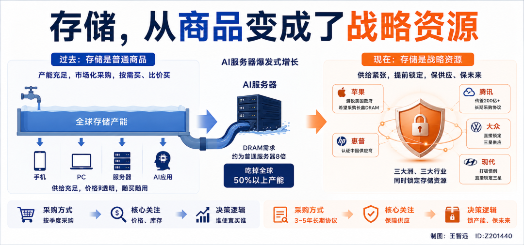
AI servers consume 8x more DRAM than standard servers, with HBM becoming a critical bottleneck.
Why It Matters
The structural shortage of memory chips will likely increase costs for AI infrastructure and potentially delay non-AI hardware production.
What To Do Next
Review your hardware infrastructure procurement strategy; consider long-term supply agreements for HBM/DDR5 to mitigate future availability risks.
Key Points
- •AI servers consume 8x more DRAM than standard servers, with HBM becoming a critical bottleneck.
- •Major memory suppliers are prioritizing high-margin AI/enterprise products over consumer electronics.
- •Procurement models have shifted from quarterly pricing to multi-year, deposit-backed capacity locking.
🧠 Deep Insight
AI-generated analysis for this event — not the original article.
🔑 Enhanced Key Takeaways
- •The transition to HBM3E and upcoming HBM4 standards is forcing manufacturers to allocate significant wafer capacity away from traditional DDR5 production, tightening supply for non-AI sectors.
- •Major memory manufacturers like SK Hynix, Samsung, and Micron have shifted capital expenditure (CapEx) toward TSV (Through-Silicon Via) packaging facilities to address the specific bottleneck in HBM assembly.
- •The 'AI premium' has led to a divergence in memory pricing, where HBM prices are estimated to be 5-7 times higher per gigabyte than standard DDR5, significantly boosting supplier margins.
- •Hyperscalers are increasingly engaging in 'co-design' partnerships with memory vendors, integrating memory architecture directly into AI accelerator roadmaps to optimize bandwidth-per-watt metrics.
- •The supply chain shift has triggered a surge in demand for advanced packaging equipment, specifically for thermocompression bonding, creating a secondary supply bottleneck for memory manufacturers.
📊 Competitor Analysis▸ Show
| Feature | HBM3E (SK Hynix) | HBM3E (Samsung) | HBM3E (Micron) |
|---|---|---|---|
| Bandwidth | Up to 1.2 TB/s | Up to 1.2 TB/s | Up to 1.2 TB/s |
| Capacity | 24GB - 36GB | 24GB - 36GB | 24GB - 36GB |
| Process Node | 10nm-class (1b) | 10nm-class (1b) | 10nm-class (1b) |
| Market Strategy | First-mover advantage | High-volume scaling | Power efficiency focus |
🛠️ Technical Deep Dive
- HBM (High Bandwidth Memory) utilizes a 3D-stacked architecture where DRAM dies are vertically interconnected using TSV (Through-Silicon Via) technology.
- The shift to HBM3E involves 8-high or 12-high stacks, requiring advanced MR-MUF (Mass Reflow Molded Underfill) or TC-NCF (Thermal Compression Non-Conductive Film) packaging to manage thermal dissipation.
- Memory wall limitations are being addressed by increasing the I/O interface width to 1024 bits per stack, significantly higher than the 64-bit interface of standard DDR5 DIMMs.
- Power efficiency is improved by lowering the operating voltage (VDD) to 1.1V, critical for maintaining thermal envelopes in dense AI server racks.
🔮 Future ImplicationsAI analysis grounded in cited sources
⏳ Timeline
Weekly AI Recap
Read this week's curated digest of top AI events →
👉Related Updates

AI-curated news aggregator. All content rights belong to original publishers.
Original source: 虎嗅 ↗
This is a summary, not the original. Read the source, or get the weekly briefing.
The weekly digest
One email a week. Unsubscribe anytime.