💰钛媒体•Stalecollected in 38m
Foundries Race to 1nm Nodes
💡1nm race starts Angstrom era – vital for AI chip future
⚡ 30-Second TL;DR
What Changed
Intense competition for 1nm wafer fabrication
Why It Matters
Enables denser AI chips, impacting compute power for large models.
What To Do Next
Track TSMC's 1nm roadmap for AI accelerator hardware planning.
Who should care:Enterprise & Security Teams
Key Points
- •Intense competition for 1nm wafer fabrication
- •Shift to Angstrom-scale (sub-1nm) processes
- •Milestone in semiconductor miniaturization
🧠 Deep Insight
AI-generated analysis for this event.
🔑 Enhanced Key Takeaways
- •The transition to 1nm and below is heavily reliant on the adoption of High-NA EUV (Extreme Ultraviolet) lithography, which is essential for achieving the necessary resolution for sub-nanometer feature sizes.
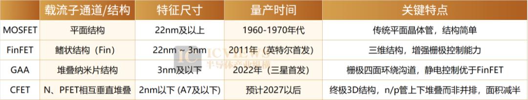
- •Foundries are shifting from FinFET to Gate-All-Around (GAA) transistor architectures, specifically nanosheet designs, as a prerequisite to overcome short-channel effects at the 2nm and 1nm nodes.
- •Backside Power Delivery Networks (BSPDN) are becoming a critical integration requirement at the 1nm node to reduce IR drop and improve power efficiency by separating signal and power routing layers.
📊 Competitor Analysis▸ Show
| Feature | TSMC (A10/A7) | Samsung Foundry (SF1.4/SF1) | Intel Foundry (14A/10A) |
|---|---|---|---|
| Transistor Architecture | GAA (Nanosheet) | GAA (MBCFET) | GAA (RibbonFET) |
| Lithography | High-NA EUV | High-NA EUV | High-NA EUV |
| Power Delivery | Backside Power | Backside Power | Backside Power |
| Status (as of 2026) | Pilot/R&D | Pilot/R&D | Pilot/R&D |
🛠️ Technical Deep Dive
- Transistor Architecture: Transition from FinFET to Gate-All-Around (GAA) FETs, utilizing nanosheets to provide superior electrostatic control over the channel.
- Lithography: Implementation of High-NA (0.55 numerical aperture) EUV scanners to enable printing of smaller features without multi-patterning, which increases complexity and cost.
- Interconnects: Integration of Backside Power Delivery Networks (BSPDN) to decouple power and signal routing, significantly reducing parasitic resistance and improving power density.
- Materials: Exploration of 2D materials (e.g., transition metal dichalcogenides like MoS2) as potential channel materials to replace silicon at sub-1nm scales to maintain performance.
🔮 Future ImplicationsAI analysis grounded in cited sources
Foundry capital expenditure will reach record highs due to High-NA EUV tool costs.
The per-unit cost of High-NA EUV scanners exceeds $350 million, forcing foundries to significantly increase investment to maintain competitive node scaling.
Yield rates for 1nm nodes will remain below 30% for the first 18 months of mass production.
The extreme complexity of GAA architecture and High-NA lithography integration historically results in prolonged yield ramp-up periods for new semiconductor nodes.
⏳ Timeline
2022-06
TSMC and Samsung initiate transition roadmaps toward GAA transistor architectures.
2023-12
Intel receives the first High-NA EUV lithography machine for R&D purposes.
2025-05
Industry-wide standardization efforts for Angstrom-era node naming conventions intensify.
📰
Weekly AI Recap
Read this week's curated digest of top AI events →
👉Related Updates

AI-curated news aggregator. All content rights belong to original publishers.
Original source: 钛媒体 ↗