Foundries Race Toward Co-Packaged Optical Connectivity
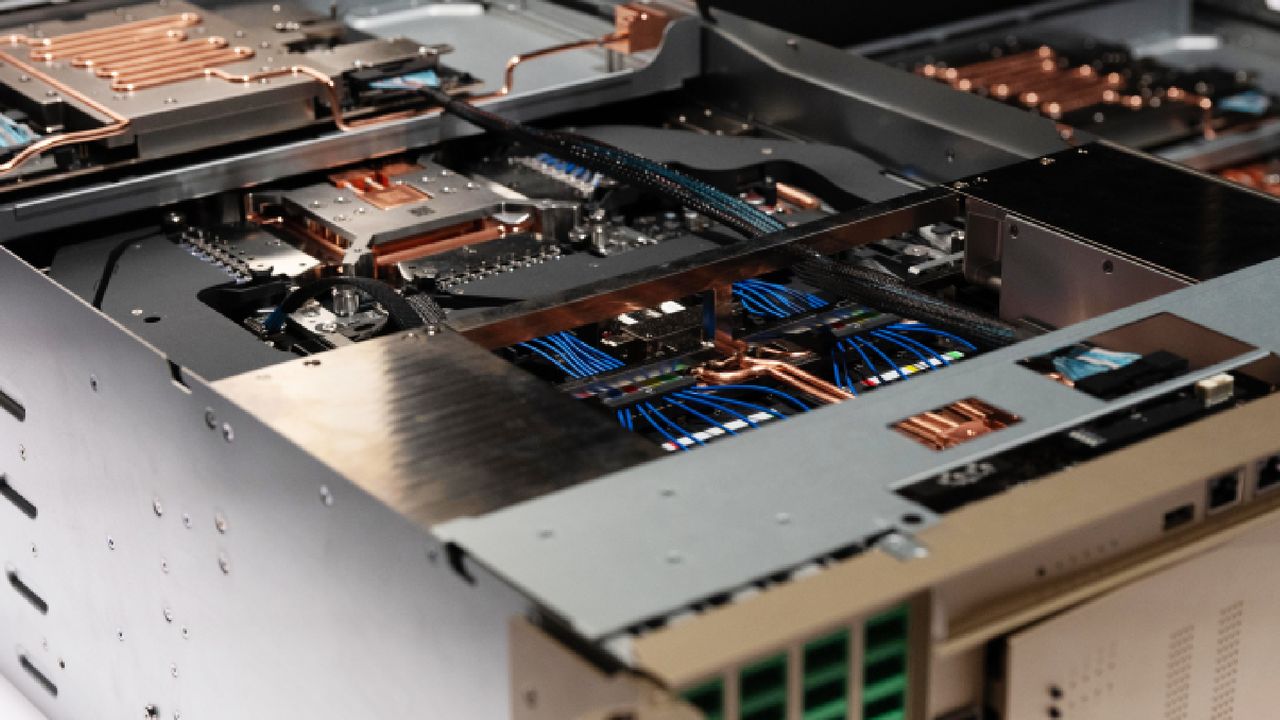
CPO may determine how future AI clusters overcome copper bandwidth limits.
30-Second TL;DR
What Changed
AI system growth is pushing traditional copper interconnects toward their performance limits.
Why It Matters
CPO could become an important interconnect direction as AI clusters require greater bandwidth and scale. Different foundry approaches may influence future accelerator, switch, and advanced-packaging supply chains.
What To Do Next
Review your next AI cluster design for CPO readiness, including optical I/O, advanced packaging, and switch-interconnect requirements.
Key Points
- •AI system growth is pushing traditional copper interconnects toward their performance limits.
- •TSMC, Intel, Samsung Foundry, and GlobalFoundries are pursuing four distinct CPO roadmaps.
- •Moving optics closer to compute could improve scale-up connectivity for next-generation AI infrastructure.
Deep Insight
AI-generated analysis for this event — not the original article.
Enhanced Key Takeaways
- •CPO integration is shifting from pluggable transceivers to silicon photonics engines integrated directly onto the substrate or interposer to reduce power consumption by up to 30-50% compared to traditional electrical I/O.
- •Thermal management remains the primary technical hurdle, as laser sources are highly sensitive to the heat generated by high-TDP AI accelerators, necessitating advanced packaging solutions like TSMC's COWOS-L.
- •Standardization efforts, such as the Universal Chiplet Interconnect Express (UCIe) and the Optical I/O Consortium, are critical to ensuring interoperability between different foundry-specific optical engines and compute dies.
- •The transition to CPO is being accelerated by the adoption of 1.6T and 3.2T Ethernet standards, where copper reach limitations make electrical signaling physically impractical for rack-scale AI clusters.
- •Foundries are increasingly utilizing heterogeneous integration, combining III-V compound semiconductors (like Indium Phosphide) for light generation with standard Silicon-on-Insulator (SOI) processes for photonics routing.
Competitor Analysis
- TSMC (CoWoS-L/CPO)
- High-end AI/HPC
- Intel (Silicon Photonics)
- Datacenter/Cloud
- Samsung (I-Cube/CPO)
- Mobile/AI/Memory
- GlobalFoundries (Fotonix)
- Automotive/Industrial
- TSMC (CoWoS-L/CPO)
- CoWoS-L/R
- Intel (Silicon Photonics)
- Embedded Bridge
- Samsung (I-Cube/CPO)
- I-Cube S/E
- GlobalFoundries (Fotonix)
- Fotonix 300mm SOI
- TSMC (CoWoS-L/CPO)
- High (Production)
- Intel (Silicon Photonics)
- High (Internal)
- Samsung (I-Cube/CPO)
- Medium (Pilot)
- GlobalFoundries (Fotonix)
- Medium (Platform)
| Feature | TSMC (CoWoS-L/CPO) | Intel (Silicon Photonics) | Samsung (I-Cube/CPO) | GlobalFoundries (Fotonix) |
|---|---|---|---|---|
| Primary Focus | High-end AI/HPC | Datacenter/Cloud | Mobile/AI/Memory | Automotive/Industrial |
| Integration Tech | CoWoS-L/R | Embedded Bridge | I-Cube S/E | Fotonix 300mm SOI |
| Maturity | High (Production) | High (Internal) | Medium (Pilot) | Medium (Platform) |
Technical Deep Dive
- Utilization of Silicon Photonics (SiPh) platforms to integrate optical modulators, waveguides, and photodetectors directly onto the silicon die.
- Implementation of micro-ring resonators to enable dense wavelength division multiplexing (DWDM) for increased bandwidth density.
- Use of advanced packaging techniques like TSMC's Chip-on-Wafer-on-Substrate (CoWoS) to bridge the gap between electrical compute dies and optical engines.
- Integration of external laser sources (ELS) to isolate heat-sensitive laser components from the high-temperature compute environment.
- Adoption of 3D stacking (TSV - Through Silicon Vias) to minimize signal latency between the optical engine and the processor.
Future ImplicationsAI analysis grounded in cited sources
Timeline
- 2021-03TSMC forms the Silicon Photonics Alliance to accelerate CPO ecosystem development.
- 2022-08GlobalFoundries launches the Fotonix platform, a 300mm silicon photonics solution.
- 2023-06Intel demonstrates integrated silicon photonics chiplets for high-bandwidth optical I/O.
- 2024-05Samsung Foundry announces the expansion of its advanced packaging roadmap to include CPO integration for AI accelerators.
- 2025-11TSMC achieves volume production readiness for CoWoS-L configurations supporting integrated optical engines.
Weekly AI Recap
Read this week's curated digest of top AI events →
AI-curated news aggregator. All content rights belong to original publishers.
Original source: Tom's Hardware ↗
This is a summary, not the original. Read the source, or get the weekly briefing.
The weekly digest
One email a week. Unsubscribe anytime.