CXMT Adopts HKMG for Next-Gen DRAM
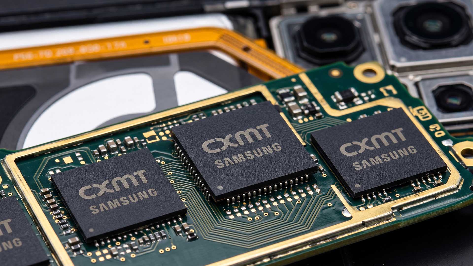
💡CXMT's HKMG adoption could reshape advanced DRAM supply for AI servers and data centers.
⚡ 30-Second TL;DR
What Changed
CXMT has implemented high-k metal gate technology in its DRAM transistors.
Why It Matters
Advanced DRAM process capabilities could strengthen CXMT's position in memory manufacturing and improve supply prospects for AI servers and other data-center systems. If the capacity projection materializes, it could also affect regional memory supply and pricing dynamics.
What To Do Next
Review your AI infrastructure roadmap and qualify multiple DRAM suppliers, including CXMT, for future accelerator-server memory availability and cost scenarios.
Key Points
- •CXMT has implemented high-k metal gate technology in its DRAM transistors.
- •HKMG is expected to help mitigate leakage problems associated with advanced process scaling.
- •The technology supports CXMT's push toward the 1a DRAM node.
- •Projected monthly capacity could reach 800,000 wafers by 2031.
🧠 Deep Insight
Background and context from public sources — not the original article. 13 sources cited.
🔑 Enhanced Key Takeaways
- •CXMT utilizes hafnium oxide (HfO₂) as the high-k dielectric material to prevent quantum tunneling leakage in sub-nanometer DRAM structures.
- •The transition to metal gate electrodes eliminates the 'polysilicon depletion' effect, which previously created electrical dead zones and reduced transistor efficiency.
- •CXMT has entered the commercial verification phase for LPDDR6 memory, specifically targeting integration with Xiaomi's upcoming flagship mobile processors.
- •The company successfully completed a major IPO on China’s STAR Market in July 2026 to fund its aggressive capacity expansion and R&D efforts.
- •CXMT is actively securing design wins with global PC OEMs and smartphone manufacturers, leveraging supply-demand imbalances to bypass geopolitical headwinds.
📊 Competitor Analysis▸ Show
| Feature | CXMT | Samsung/Micron |
|---|---|---|
| HKMG Adoption | 2026 (1a node) | ~2020-2021 (1z node) |
| Market Status | Emerging/Domestic | Established/Global |
| Node Maturity | 1a (Transitioning) | 1b/1c (Mass Production) |
| Pricing | Competitive/Aggressive | Premium/Market-driven |
🛠️ Technical Deep Dive
- Material Science: Implementation of hafnium-based high-k dielectrics to replace silicon dioxide insulators.
- Gate Architecture: Replacement of traditional polysilicon gates with metal stacks to mitigate depletion effects.
- Scaling Strategy: Transitioning from legacy nodes to the 1a (1-alpha) process node to increase bit density.
- Power Efficiency: Reduction of gate leakage current, enabling lower voltage operation for LPDDR6 applications.
🔮 Future ImplicationsAI analysis grounded in cited sources
⏳ Timeline
📎 Sources (13)
Factual claims are grounded in the sources below. Forward-looking analysis is AI-generated interpretation.
Weekly AI Recap
Read this week's curated digest of top AI events →
👉Related Updates


AI-curated news aggregator. All content rights belong to original publishers.
Original source: cnBeta (Full RSS) ↗
This is a summary, not the original. Read the source, or get the weekly briefing.
Weekly AI briefing
One email a week. Unsubscribe anytime.