China’s Chip Gap Shrinks—But Wafer Size Matters
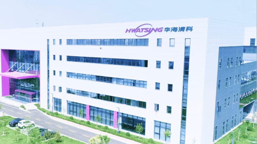
A new integrated metrology system reveals both China’s equipment progress and its remaining AI-chip manufacturing gap.
30-Second TL;DR
What Changed
Hwatsing Technology introduced a metrology system for six-inch wafers.
Why It Matters
Better in-process metrology could improve yield control and process consistency for domestic chip manufacturers. For AI infrastructure, however, the wafer size suggests this is more relevant to foundational equipment capability than to immediate cutting-edge GPU production.
What To Do Next
Track Hwatsing’s support for eight- and twelve-inch wafers before considering it for high-volume AI-chip manufacturing equipment.
Key Points
- •Hwatsing Technology introduced a metrology system for six-inch wafers.
- •The system is built directly into the CMP workflow for in-process measurement.
- •China’s six-inch focus indicates progress in equipment integration but continued lag in advanced wafer manufacturing.
Deep Insight
AI-generated analysis for this event — not the original article.
Enhanced Key Takeaways
- •Hwatsing Technology, based in Tianjin, is a key beneficiary of China's 'Big Fund' (China Integrated Circuit Industry Investment Fund) aimed at reducing reliance on foreign semiconductor equipment.
- •The integration of metrology into Chemical Mechanical Polishing (CMP) is a critical step toward 'smart manufacturing' in China, as it reduces the cycle time for defect detection and process correction.
- •While six-inch wafers are considered legacy technology for logic chips, they remain essential for power semiconductors, MEMS, and analog devices, which are high-growth areas for China's domestic automotive and industrial sectors.
- •Hwatsing has historically faced stiff competition from global leaders like Applied Materials and Lam Research, which dominate the high-end CMP market with integrated metrology solutions.
- •The development of this system aligns with China's broader strategy to achieve self-sufficiency in 'mature node' manufacturing, where the country is aggressively expanding capacity to dominate the global supply of non-leading-edge chips.
Competitor Analysis
- Hwatsing Technology (China)
- Emerging (6-inch focus)
- Applied Materials (Global)
- Mature (300mm/12-inch)
- Lam Research (Global)
- Mature (300mm/12-inch)
- Hwatsing Technology (China)
- Domestic/Legacy Nodes
- Applied Materials (Global)
- Global/Leading-Edge
- Lam Research (Global)
- Global/Leading-Edge
- Hwatsing Technology (China)
- Competitive/Subsidized
- Applied Materials (Global)
- Premium
- Lam Research (Global)
- Premium
- Hwatsing Technology (China)
- High defect sensitivity for 6-inch
- Applied Materials (Global)
- Industry standard for 300mm
- Lam Research (Global)
- Industry standard for 300mm
| Feature | Hwatsing Technology (China) | Applied Materials (Global) | Lam Research (Global) |
|---|---|---|---|
| CMP Metrology Integration | Emerging (6-inch focus) | Mature (300mm/12-inch) | Mature (300mm/12-inch) |
| Primary Market | Domestic/Legacy Nodes | Global/Leading-Edge | Global/Leading-Edge |
| Pricing | Competitive/Subsidized | Premium | Premium |
| Benchmark | High defect sensitivity for 6-inch | Industry standard for 300mm | Industry standard for 300mm |
Technical Deep Dive
- System utilizes in-situ monitoring sensors to track wafer thickness and material removal rates in real-time during the polishing process.
- Employs optical-based metrology modules embedded directly into the CMP platen or carrier head assembly.
- Designed to interface with existing legacy CMP platforms to upgrade throughput and yield without requiring a full system replacement.
- Focuses on reducing the 'wafer-to-wafer' variation by providing closed-loop feedback to the polishing parameters.
Future ImplicationsAI analysis grounded in cited sources
Timeline
- 2013-01Hwatsing Technology is founded in Tianjin, China, focusing on CMP equipment development.
- 2018-05Hwatsing achieves a breakthrough in 12-inch CMP equipment, marking a shift toward larger wafer capabilities.
- 2022-12Company completes a significant funding round to accelerate R&D in advanced semiconductor manufacturing equipment.
- 2026-08Hwatsing announces the integration of metrology systems into six-inch CMP workflows.
Weekly AI Recap
Read this week's curated digest of top AI events →
Related Updates



AI-curated news aggregator. All content rights belong to original publishers.
Original source: The Next Web (TNW) ↗
This is a summary, not the original. Read the source, or get the weekly briefing.
The weekly digest
One email a week. Unsubscribe anytime.