China Accelerates AI Chip Packaging Expansion
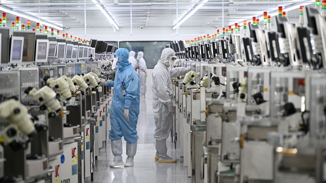
💡China’s AI-driven packaging buildout could reshape accelerator supply, costs, and regional sourcing options.
⚡ 30-Second TL;DR
What Changed
China’s three leading outsourced chip packaging companies announced multibillion-dollar capacity investments.
Why It Matters
Expanded packaging capacity could reduce bottlenecks for AI accelerators and strengthen China’s domestic semiconductor ecosystem. For AI companies, it may eventually improve regional supply resilience, although qualification timelines and access to advanced packaging technologies remain important constraints.
What To Do Next
Map your AI hardware roadmap against OSAT dependencies and begin qualifying alternative packaging partners, including JCET, Tongfu Microelectronics, and Huatian Technology.
Key Points
- •China’s three leading outsourced chip packaging companies announced multibillion-dollar capacity investments.
- •AI demand is increasing pressure on advanced semiconductor assembly and testing capacity.
- •Strong first-half profits are giving Chinese chip-packaging firms more room to fund expansion.
- •The buildout supports Beijing’s broader goal of reducing reliance on overseas semiconductor supply chains.
🧠 Deep Insight
Background and context from public sources — not the original article. 9 sources cited.
🔑 Enhanced Key Takeaways
- •China has initiated nearly 10 major advanced packaging projects totaling 400 billion yuan between May and July 2026, specifically targeting 2.5D/3D integration and Chiplet architectures.
- •Chinese OSAT firms are pivoting toward glass substrate adoption to bypass silicon-based thermal and transmission bottlenecks in high-performance AI computing.
- •Goldman Sachs estimates China's domestic 7nm-and-below wafer supply will grow at a 46% CAGR, aiming to reduce the domestic supply shortfall from 92% in 2025 to 34% by 2035.
- •The industry is aggressively integrating optical interconnects and 3D stacking to maintain AI performance gains as a workaround for restricted access to EUV lithography equipment.
- •Domestic foundries like SMIC are shifting focus toward packaging integration to maximize yields on existing advanced process nodes, directly supporting the infrastructure needs of local AI chip designers.
📊 Competitor Analysis▸ Show
| Feature | Chinese OSATs (JCET/Tongfu/Huatian) | Global Leaders (TSMC/ASE/Amkor) |
|---|---|---|
| Advanced Packaging | Rapidly scaling 2.5D/3D/Chiplet | Industry standard (CoWoS/InFO) |
| Lithography Access | Restricted (Duv-focused) | Unrestricted (EUV access) |
| Strategic Focus | Domestic self-sufficiency | Global high-performance supply chain |
| Market Position | High-volume, cost-competitive | Premium, high-margin, high-complexity |
🛠️ Technical Deep Dive
- 2.5D/3D Integration: Utilization of interposers and TSV (Through-Silicon Via) technology to stack logic and memory dies.
- Glass Substrates: Implementation of glass-core substrates to improve signal integrity and thermal stability for high-density AI chips.
- Chiplet Architecture: Modular design approach allowing the combination of different process nodes into a single package to optimize cost and yield.
- Optical Interconnects: Integration of silicon photonics to facilitate high-speed data transfer between chiplets, reducing latency in AI data centers.
🔮 Future ImplicationsAI analysis grounded in cited sources
⏳ Timeline
📎 Sources (9)
Factual claims are grounded in the sources below. Forward-looking analysis is AI-generated interpretation.
Weekly AI Recap
Read this week's curated digest of top AI events →
👉Related Updates
AI-curated news aggregator. All content rights belong to original publishers.
Original source: SCMP Technology ↗
This is a summary, not the original. Read the source, or get the weekly briefing.
Weekly AI briefing
One email a week. Unsubscribe anytime.