🇨🇳cnBeta (Full RSS)•Stalecollected in 63m
Atomic Imaging Spots 'Mouse Bite' Chip Defects
💡Reveals hidden chip flaws hurting AI accelerator yields.
⚡ 30-Second TL;DR
What Changed
First atomic-scale imaging of hidden chip defects
Why It Matters
Enhances chip manufacturing reliability, critical for scaling AI hardware like GPUs amid supply constraints.
What To Do Next
Adopt atomic imaging tools in your AI chip fab pipeline for defect analysis.
Who should care:Researchers & Academics
🧠 Deep Insight
Web-grounded analysis with 7 cited sources.
🔑 Enhanced Key Takeaways
- •The technique employs electron ptychography, a computational imaging method that reconstructs high-resolution 3D atomic structures from electron microscope data[1][2][3].
- •Collaboration includes TSMC and ASM, applying the method to inspect defects in real transistor devices[2].
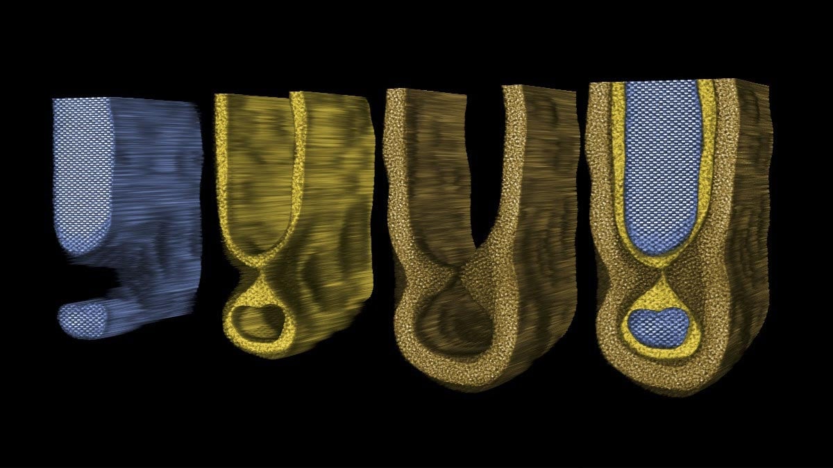
- •Defects termed 'mouse bites' appear as missing atomic columns in the chip lattice, potentially causing performance failures[1][3][4].
- •'Mouse bites' were visualized in 3D at atomic resolution, revealing irregularities previously undetectable by standard methods[1][2].
🛠️ Technical Deep Dive
- •Utilizes electron ptychography: Overlapping electron probe scans are computationally reconstructed to achieve sub-angstrom resolution imaging of atomic structures[1][2][3].
- •Applied to advanced transistors: Inspects gate-all-around (GAA) or FinFET structures where atomic defects disrupt electrical performance[2].
- •'Mouse bites' are atomic-scale voids: Irregular missing atoms or lattice disruptions, sized ~1-2 atomic spacings, observed in 3D electron tomography[1][3].
- •Imaging resolution: ~40 pm (picometers), enabling direct visualization inside intact chip layers without destructive sectioning[1][2].
🔮 Future ImplicationsAI analysis grounded in cited sources
Chip yields improve by 5-10% in sub-2nm nodes through defect identification and process correction.
Electron ptychography adopted industry-wide by 2028 for routine defect metrology.
Collaboration with TSMC and ASM demonstrates scalability for production inspection of advanced logic devices[2].
⏳ Timeline
2025-07
Cornell–MIT electron ptychography workshop held to advance defect imaging techniques[5].
2026-03
Cornell team publishes first atomic-scale 3D imaging of 'mouse bite' defects in chips[1].
📎 Sources (7)
Factual claims are grounded in the sources below. Forward-looking analysis is AI-generated interpretation.
- news.cornell.edu — Electron Microscopy Shows Mouse Bite Defects Semiconductors
- semiengineering.com — Research Bits March 3
- scienceblog.com — Electron Ptychography Reveals Atomic Mouse Bite Defects Inside Computer Chips
- scitechdaily.com
- academic.oup.com — Qaaf111
- news.cornell.edu — Archive
- techxplore.com — 2026 01 Supersonic Defy Year Metal Strength
📰
Weekly AI Recap
Read this week's curated digest of top AI events →
👉Related Updates


AI-curated news aggregator. All content rights belong to original publishers.
Original source: cnBeta (Full RSS) ↗