Source钛媒体•Stalecollected in 12m
ASML Sparks Global AI Infra Storm
#chip-supply#ai-infra#risk-analysisasml-lithographyasml
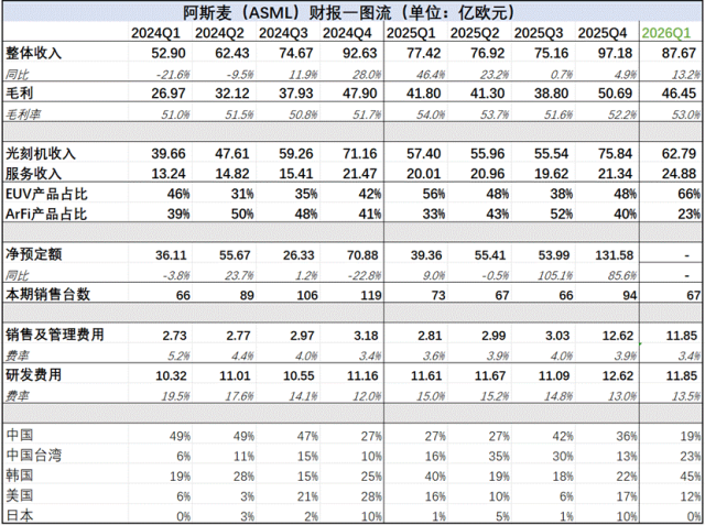
💡ASML moves threaten AI chip supply chain—key risks for model trainers
⚡ 30-Second TL;DR
What Changed
Lithography king initiates key action
Why It Matters
ASML's developments could bottleneck or boost AI chip production, affecting training costs for large models.
What To Do Next
Review ASML's latest earnings call for AI chip supply projections.
Who should care:Enterprise & Security Teams
Key Points
- •Lithography king initiates key action
- •Impacts global AI infrastructure buildup
- •Examines four overlooked risk variables
- •Beyond standard market consensus views
🧠 Deep Insight
AI-generated analysis for this event — not the original article.
🔑 Enhanced Key Takeaways
- •ASML has shifted its strategic focus toward High-NA EUV (0.55 NA) lithography systems, which are essential for manufacturing sub-2nm process nodes required for next-generation AI accelerators.
- •The 'storm' refers to the supply chain bottleneck created by the extreme cost and complexity of High-NA EUV machines, forcing major chipmakers like TSMC, Intel, and Samsung to re-evaluate their capital expenditure timelines.
- •Geopolitical export controls on advanced lithography equipment have created a bifurcated global AI infrastructure market, complicating the scaling efforts of non-Western AI hardware developers.
📊 Competitor Analysis▸ Show
| Feature | ASML (High-NA EUV) | Canon (Nanoimprint) | Nikon (ArF Immersion) |
|---|---|---|---|
| Technology | Extreme Ultraviolet | Nanoimprint Lithography | Deep Ultraviolet |
| Resolution | < 8nm (sub-2nm nodes) | ~10-15nm | > 38nm |
| Primary Use | Leading-edge Logic/AI | Memory/Specialized | Mature Nodes/Legacy |
| Market Position | Monopoly (Leading-edge) | Niche/Alternative | Mid-range/Legacy |
🛠️ Technical Deep Dive
- •High-NA EUV utilizes a 0.55 numerical aperture lens, an increase from the 0.33 NA used in standard EUV systems, allowing for higher resolution patterning.
- •The system requires a new anamorphic lens design to manage the increased light collection angle, which necessitates a reduction in the field size of the reticle by half.
- •Implementation requires advanced photoresist materials with higher sensitivity to maintain throughput, as the increased NA impacts depth-of-focus constraints.
🔮 Future ImplicationsAI analysis grounded in cited sources
High-NA EUV adoption will delay the transition to 1.4nm nodes for most foundries.
The extreme cost per wafer and the technical challenges of anamorphic field stitching will force manufacturers to extend the life of existing 2nm-class processes.
ASML's revenue concentration will shift heavily toward a small cohort of hyperscaler-aligned foundries.
Only companies with massive AI-driven capital budgets can afford the $350M+ price tag per High-NA machine, limiting the customer base.
⏳ Timeline
2023-12
ASML ships the first High-NA EUV system (EXE:5000) to Intel.
2024-04
ASML reports first-quarter earnings showing a significant backlog of High-NA orders.
2025-07
ASML announces expanded production capacity for the EXE:5200 series to meet AI demand.
📰
Weekly AI Recap
Read this week's curated digest of top AI events →
👉Related Updates



AI-curated news aggregator. All content rights belong to original publishers.
Original source: 钛媒体 ↗
This is a summary, not the original. Read the source, or get the weekly briefing.
The weekly digest
One email a week. Unsubscribe anytime.