ASML considers price hikes for advanced chipmaking tools
💡Rising equipment costs at ASML could signal higher prices for the next generation of AI-specialized silicon.
⚡ 30-Second TL;DR
What Changed
ASML planning price increases for lithography tools
Why It Matters
Higher equipment costs may eventually trickle down to increased prices for AI chips, impacting the total cost of ownership for AI model training.
What To Do Next
Monitor semiconductor capital expenditure trends as they directly correlate with future AI compute pricing.
Key Points
- •ASML planning price increases for lithography tools
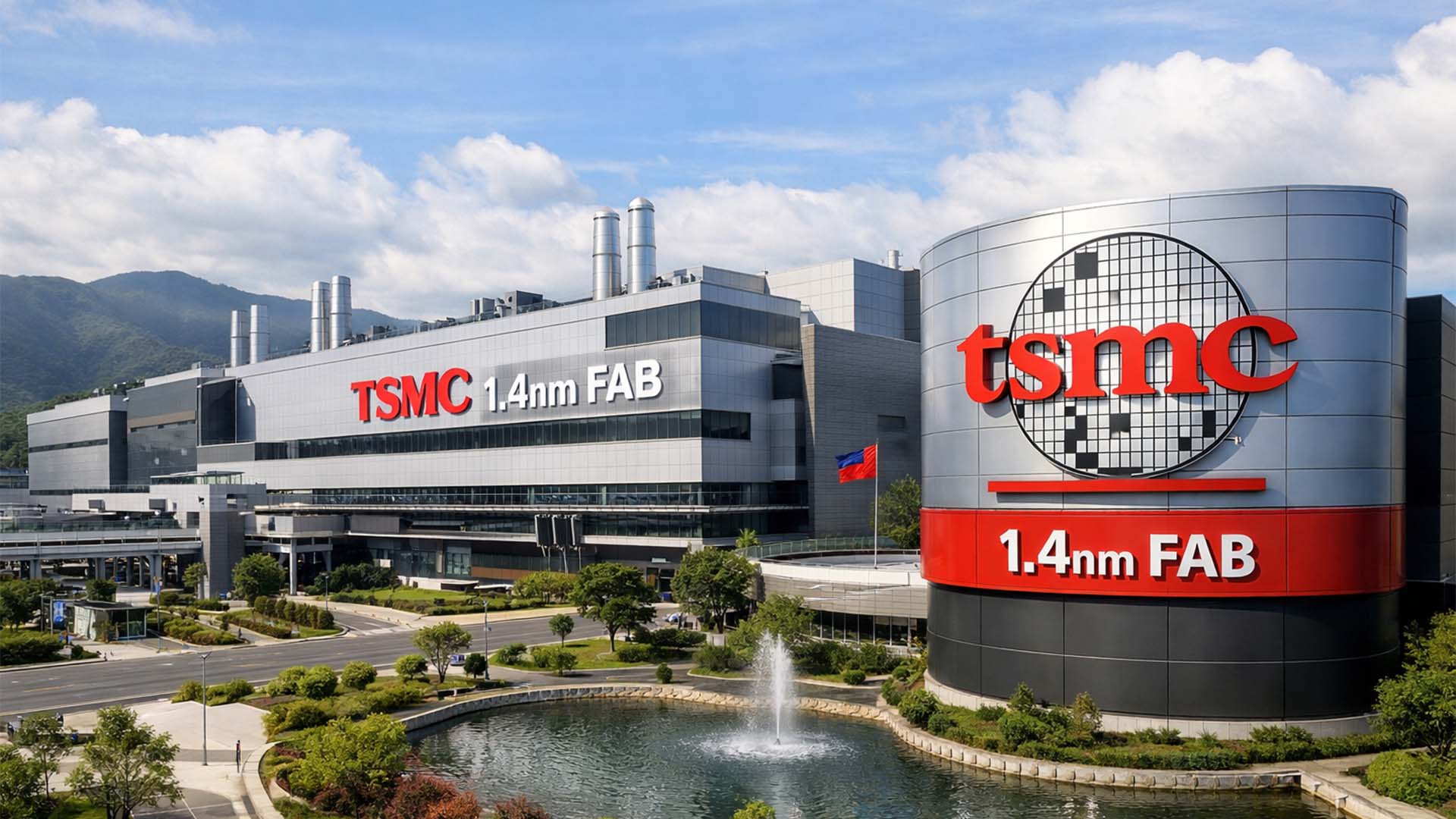
- •Potential conflict with major client TSMC
- •Reflects rising costs in semiconductor manufacturing equipment
🧠 Deep Insight
AI-generated analysis for this event.
🔑 Enhanced Key Takeaways
- •ASML's pricing strategy is heavily influenced by the massive R&D expenditure required for High-NA EUV (Extreme Ultraviolet) lithography systems, which cost over $350 million per unit.
- •The potential price hikes are occurring against a backdrop of geopolitical export restrictions that have limited ASML's ability to sell advanced tools to the Chinese market, impacting overall revenue diversification.
- •TSMC's bargaining power is significant as they are the primary adopter of ASML's most advanced EXE:5200 High-NA systems, creating a symbiotic but tense dependency.
- •Rising costs are partially driven by supply chain inflation for specialized components, such as the high-precision mirrors and laser sources required for EUV systems.
- •ASML has signaled that the transition to next-generation hyper-NA EUV technology will require even greater capital investment from customers, setting a precedent for long-term price escalation.
📊 Competitor Analysis▸ Show
| Feature | ASML | Canon | Nikon |
|---|---|---|---|
| Primary Tech | EUV / High-NA EUV | Nanoimprint (NIL) | ArF Immersion / DUV |
| Market Position | Monopoly in EUV | Niche / Emerging | Legacy / Mid-range |
| Pricing Strategy | Premium / High-Margin | Cost-effective / Alternative | Competitive / Value-focused |
| Resolution | Sub-2nm capability | Sub-5nm (theoretical) | 7nm+ nodes |
🛠️ Technical Deep Dive
- High-NA EUV (0.55 NA) systems utilize a larger numerical aperture to achieve higher resolution, enabling printing of features below 8nm in a single exposure.
- The anamorphic lens design in High-NA systems requires a 4x magnification in one direction and 8x in the other to optimize image fidelity.
- EUV light sources operate at 13.5nm wavelength, generated by hitting tin droplets with high-power CO2 lasers, a process that is extremely energy-intensive.
- ASML's EXE:5000 and EXE:5200 models represent the current pinnacle of lithography, requiring specialized cleanroom infrastructure due to their massive physical footprint.
🔮 Future ImplicationsAI analysis grounded in cited sources
⏳ Timeline
Weekly AI Recap
Read this week's curated digest of top AI events →
👉Related Updates
Same topic
Explore #semiconductor
Same product
More on asml-chipmaking-equipment
Same source
Latest from Bloomberg Technology

Sugon Establishes New Information Industry Subsidiary in Guangxi
TSMC Exec Accused of Stealing Trade Secrets for Intel
Hyundai Moves to Fully Acquire Boston Dynamics
EU and India Initiate Horizon Research Program Partnership
AI-curated news aggregator. All content rights belong to original publishers.
Original source: Bloomberg Technology ↗