🌍The Next Web (TNW)•Freshcollected in 20m
ASML accelerates EUV machine production by 30%
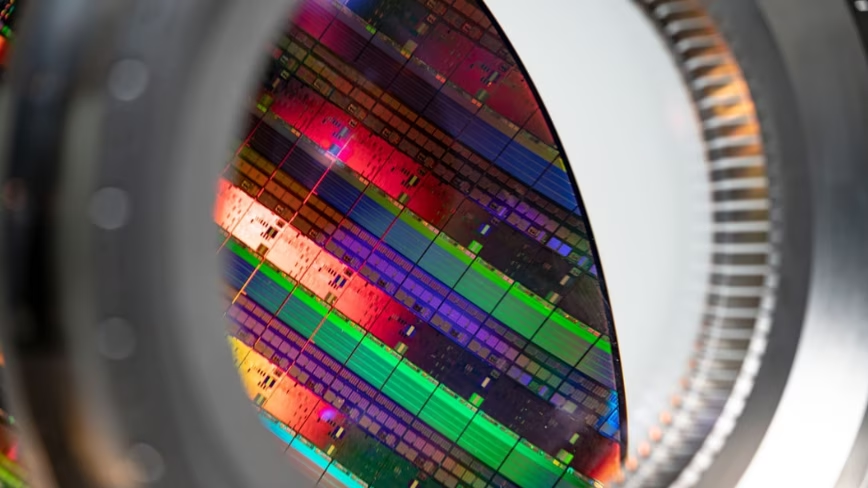
💡ASML's production speed directly dictates the global supply of advanced AI chips.
⚡ 30-Second TL;DR
What Changed
ASML is cutting EUV machine production cycle time by one-third
Why It Matters
Faster EUV production could alleviate the global AI chip bottleneck, allowing foundries to scale advanced node manufacturing more quickly.
What To Do Next
Track lead times for advanced node chips (3nm/2nm) as ASML's production efficiency improves.
Who should care:Enterprise & Security Teams
Key Points
- •ASML is cutting EUV machine production cycle time by one-third
- •AI demand is currently outstripping existing production capacity
- •Efficiency gains focus on clean room assembly and testing processes
🧠 Deep Insight
AI-generated analysis for this event.
🔑 Enhanced Key Takeaways
- •ASML is leveraging 'modular assembly' techniques to allow parallel testing of sub-modules, significantly reducing the final integration phase in the clean room.
- •The production acceleration is specifically targeting the High-NA EUV (EXE:5200) systems, which are critical for sub-2nm process nodes.
- •Supply chain bottlenecks for critical components, such as the Zeiss optical systems and Cymer light sources, have been mitigated through multi-year strategic inventory buffering.
- •The 30% cycle time reduction is expected to increase ASML's annual EUV output capacity by approximately 10-15 units by the end of 2027.
- •ASML has implemented AI-driven predictive maintenance and digital twin simulations to identify and resolve assembly line micro-stoppages in real-time.
📊 Competitor Analysis▸ Show
| Feature | ASML (EUV) | Canon (NIL) | Nikon (ArFi/EUV) |
|---|---|---|---|
| Lithography Method | Extreme Ultraviolet | Nanoimprint Lithography | DUV / EUV (R&D) |
| Resolution | < 8nm (High-NA) | < 10nm | > 30nm (DUV) |
| Primary Market | Leading-edge Logic/Memory | Low-cost/Specialized Logic | Mature Nodes / Memory |
🛠️ Technical Deep Dive
- High-NA EUV systems utilize a 0.55 numerical aperture lens, an increase from the 0.33 NA used in previous Low-NA models.
- The reduction in cycle time is achieved by transitioning from a serial 'build-and-test' workflow to a 'parallel modular' workflow.
- Integration of advanced metrology sensors allows for in-situ calibration, reducing the time required for post-assembly optical alignment.
- The process utilizes a new generation of pellicles with higher thermal resistance to support the increased power density of the EUV light source.
🔮 Future ImplicationsAI analysis grounded in cited sources
Foundry lead times for 2nm chips will decrease by Q2 2027.
Increased throughput of EUV machines directly expands the capacity for leading-edge wafer starts at major foundries.
ASML's gross margin will expand due to improved manufacturing efficiency.
Reducing cycle time lowers the overhead costs per machine and allows for higher revenue recognition within a single fiscal year.
⏳ Timeline
2010-04
ASML ships the first pre-production EUV lithography system (NXE:3100).
2018-07
ASML reaches the milestone of 30 EUV systems shipped cumulatively.
2023-12
ASML delivers the first High-NA EUV (EXE:5000) pilot system to Intel.
2025-05
ASML announces the transition to high-volume manufacturing (HVM) for High-NA EUV systems.
📰
Weekly AI Recap
Read this week's curated digest of top AI events →
👉Related Updates



AI-curated news aggregator. All content rights belong to original publishers.
Original source: The Next Web (TNW) ↗