AI-Driven PCB Nears the Cliff
AI server PCB demand is surging, but today’s capacity boom could become tomorrow’s supply glut.
30-Second TL;DR
What Changed
AI server PCB market space is projected to exceed 900 billion yuan in 2026, more than doubling year over year.
Why It Matters
AI infrastructure builders may face continued PCB cost and lead-time pressure in the near term. However, if standardized capacity scales before AI server demand maintains its current growth rate, hardware margins and supplier valuations could be vulnerable to a sharp rebalancing.
What To Do Next
Track TrendForce AI server shipment forecasts alongside supplier capex and PCB lead times, then stress-test your hardware roadmap against a 2027 capacity oversupply scenario.
Key Points
- •AI server PCB market space is projected to exceed 900 billion yuan in 2026, more than doubling year over year.
- •Capital expenditure by nine leading PCB companies reached 26.7 billion yuan in 2025, up 111%, with annualized growth accelerating further in early 2026.
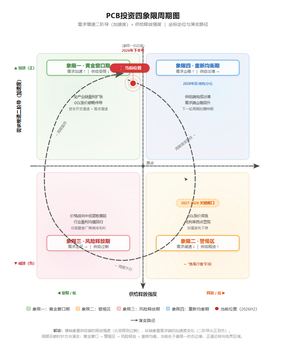
- •New PCB production lines typically require 18–24 months for construction, certification, and yield ramp-up, suggesting substantial capacity may arrive around 2027.
- •Electronic cloth prices rose 118%–165% year to date, but the monthly acceleration of copper-clad laminate price increases is beginning to moderate.
- •Highly advanced 40–60-layer AI server backplanes remain supply-constrained, while standardized 20–30-layer boards could scale faster than market expectations.
Deep Insight
AI-generated analysis for this event — not the original article.
Enhanced Key Takeaways
- •The surge in demand for high-layer count PCBs is specifically tied to the transition from OAM (Open Accelerator Module) to larger, more complex GPU cluster architectures requiring ultra-low-loss materials like PTFE and modified epoxy resins.
- •Major PCB manufacturers are increasingly adopting 'AI-native' manufacturing execution systems (MES) to manage the yield volatility inherent in producing 40+ layer boards, which currently suffer from higher-than-average lamination defects.
- •Upstream supply chain bottlenecks are shifting from raw copper foil to specialized glass fiber yarns, where production capacity is highly concentrated among a few global suppliers, creating a 'chokepoint' effect for CCL makers.
- •Regional policy shifts in Southeast Asia and Mexico are attracting PCB manufacturers to relocate assembly lines to mitigate geopolitical risks, adding a layer of 'relocation capex' on top of the 'capacity expansion capex' mentioned in the article.
- •The industry is seeing a divergence in profitability: while high-layer AI boards command premium margins, the commoditization of lower-layer boards used in peripheral AI infrastructure is leading to price wars among Tier-2 and Tier-3 suppliers.
Technical Deep Dive
- High-layer count PCBs (40-60 layers) utilize advanced materials with ultra-low dielectric constant (Dk) and dissipation factor (Df) to maintain signal integrity at high frequencies (112G/224G SerDes).
- Manufacturing processes involve sequential lamination cycles, which increase the risk of registration errors and thermal stress-induced delamination.
- The use of laser direct imaging (LDI) is becoming mandatory for fine-line patterning (sub-50 micron) required for high-density interconnects in AI server backplanes.
- Thermal management in these boards often requires embedded copper coins or heavy copper layers to dissipate heat generated by high-TDP (Thermal Design Power) AI accelerators.
Future ImplicationsAI analysis grounded in cited sources
Timeline
- 2024-03Initial surge in AI server demand triggers widespread PCB capacity expansion announcements.
- 2024-11Copper-clad laminate (CCL) prices begin a sustained upward trend due to raw material shortages.
- 2025-06Major PCB manufacturers report record-breaking capital expenditure for AI-specific production lines.
- 2026-02Industry reports indicate the first signs of price acceleration moderation for standard CCL products.
Weekly AI Recap
Read this week's curated digest of top AI events →
AI-curated news aggregator. All content rights belong to original publishers.
Original source: 虎嗅 ↗
This is a summary, not the original. Read the source, or get the weekly briefing.
The weekly digest
One email a week. Unsubscribe anytime.