來源cnBeta (Full RSS)•較早收集於 2h
超小型「納米雷射器」問世 有望重塑未來電腦晶片
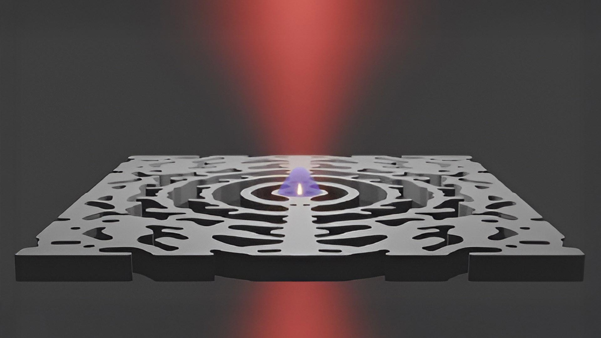
#photonics#nano-laser#photonic-chipsdtu-nanolaserdtu
💡每晶片數千納米雷射器可大幅降低AI硬體功耗需求。
⚡ 30 秒速覽
有什麼變化
丹麥技術大學團隊在半導體薄膜中建構納米雷射器
為什麼重要
此進展推動光子運算,有潛力實現更密集低功耗AI加速器,適用資料中心。可能加速AI訓練與推論工作負載擴展。
下一步行動
檢閱丹麥技術大學納米雷射器論文,用於原型設計AI晶片光子互連。
誰應關注:Researchers & Academics
關鍵要點
- •丹麥技術大學團隊在半導體薄膜中建構納米雷射器
- •實現晶片內光子取代電子資料傳輸
- •支援單一微晶片整合數千個單位
- •提升速度並大幅降低功耗
🧠 深度解析
本篇為 AI 生成分析,非原文內容。
🔑 增強重點摘要
- •The DTU nano laser utilizes a photonic crystal cavity design, which allows for extreme light confinement within a sub-wavelength volume, overcoming the traditional diffraction limit.
- •The research team successfully demonstrated room-temperature continuous-wave operation, a critical hurdle for practical integration into commercial CMOS manufacturing processes.
- •The integration approach leverages a heterogeneous integration technique, bonding III-V semiconductor materials onto silicon-on-insulator (SOI) wafers to combine light-emitting efficiency with silicon's scalability.
🛠️ 技術深入
- Cavity Type: Photonic crystal nanobeam cavity.
- Material Platform: Indium Phosphide (InP) membrane bonded to Silicon-on-Insulator (SOI).
- Footprint: Sub-micron scale, enabling high-density integration.
- Operating Mode: Continuous-wave (CW) operation at room temperature.
- Coupling: Efficient evanescent coupling to silicon waveguides for on-chip signal routing.
🔮 前景展望基於引用來源的 AI 分析
Photonic interconnects will replace copper traces for intra-chip communication by 2030.
The ability to integrate thousands of nano lasers directly onto silicon wafers removes the primary bottleneck of energy-intensive electrical data movement.
Data center power consumption will drop by at least 30% due to optical chip-to-chip interconnects.
Replacing electrical signaling with low-power photonic links eliminates the need for power-hungry electrical-to-optical conversions at every stage of data transmission.
⏳ 時間線
2023-05
DTU researchers publish initial findings on high-efficiency light confinement in semiconductor membranes.
2025-02
Successful demonstration of room-temperature continuous-wave operation for the nano laser prototype.
📰
AI 週報
閱讀本週精選 AI 大事摘要 →
👉相關動態
AI 策展新聞聚合。所有內容版權歸原始發布者所有。
原始來源: cnBeta (Full RSS) ↗
每週電子報
每週一封,可隨時退訂。