🇨🇳cnBeta (Full RSS)•Stalecollected in 13h
YMTC Phase 3 Fab Mass Production H2
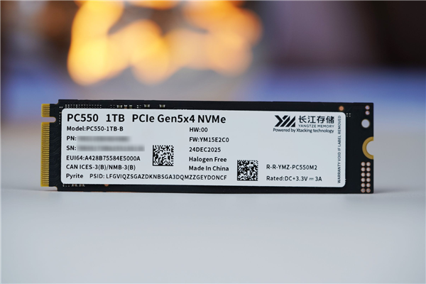
💡YMTC NAND capacity tops SK Hynix, boosting AI infra storage supply.
⚡ 30-Second TL;DR
What Changed
Phase 3 fab completing key equipment installation
Why It Matters
Expands global NAND supply, potentially easing shortages for AI data centers and lowering storage costs amid surging demand.
What To Do Next
Benchmark YMTC high-density NAND for AI training dataset storage scalability.
Who should care:Enterprise & Security Teams
Key Points
- •Phase 3 fab completing key equipment installation
- •H2 start of high-layer-count NAND mass production
- •Total YMTC capacity to exceed SK Hynix
- •Positions YMTC as global NAND third-largest
🧠 Deep Insight
AI-generated analysis for this event.
🔑 Enhanced Key Takeaways
- •YMTC's expansion is heavily constrained by US export controls, specifically the October 2022 BIS restrictions that limit the import of advanced semiconductor manufacturing equipment for NAND production exceeding 128 layers.
- •The Phase 3 facility is reportedly utilizing domestic Chinese equipment suppliers and repurposed older-generation tools to circumvent international sanctions, impacting overall yield rates compared to global peers.
- •Industry analysts note that YMTC's aggressive capacity expansion is primarily driven by Chinese government subsidies and the 'Big Fund' (China Integrated Circuit Industry Investment Fund) to achieve domestic self-sufficiency in memory storage.
📊 Competitor Analysis▸ Show
| Feature | YMTC (Phase 3) | Samsung Electronics | SK Hynix | Micron Technology |
|---|---|---|---|---|
| NAND Layer Count | ~232+ (Xtacking 3.0) | 300+ (V-NAND) | 300+ (4D NAND) | 232+ (Replacement Gate) |
| Market Strategy | Domestic/Cost-focused | Premium/High-density | High-performance/AI | Enterprise/Data Center |
| Supply Chain | Restricted (Domestic focus) | Global/Diversified | Global/Diversified | Global/Diversified |
🛠️ Technical Deep Dive
- •Architecture: Utilizes proprietary 'Xtacking' technology, which separates the peripheral CMOS logic circuitry from the NAND array wafer, allowing for independent optimization of both.
- •Interconnect: Employs high-density vertical interconnect access (VIA) to bond the CMOS wafer to the array wafer, enabling higher I/O speeds compared to traditional monolithic NAND designs.
- •Scaling: The Phase 3 production focus is on high-layer-count 3D NAND, aiming to push beyond 232 layers using advanced etching and deposition processes despite equipment limitations.
🔮 Future ImplicationsAI analysis grounded in cited sources
YMTC will face significant margin pressure due to yield volatility.
Reliance on non-leading-edge equipment for high-stack NAND production typically results in lower wafer yields and higher per-unit manufacturing costs compared to competitors.
Global NAND market share will see increased price competition in the commodity segment.
The addition of massive capacity from Phase 3 will likely force YMTC to aggressively price its products to gain market share, potentially triggering a price war in the lower-tier NAND market.
⏳ Timeline
2016-07
Yangtze Memory Technologies Co. (YMTC) is established in Wuhan, China.
2018-08
YMTC announces its proprietary Xtacking architecture at Flash Memory Summit.
2020-04
YMTC begins mass production of 128-layer 3D NAND flash memory.
2022-10
US Department of Commerce adds YMTC to the Entity List, restricting access to advanced US semiconductor technology.
2024-07
YMTC initiates mass production ramp-up at the Wuhan Phase 3 facility.
📰
Weekly AI Recap
Read this week's curated digest of top AI events →
👉Related Updates


AI-curated news aggregator. All content rights belong to original publishers.
Original source: cnBeta (Full RSS) ↗