YMTC-Backed Fund Bets on FD-SOI Chips
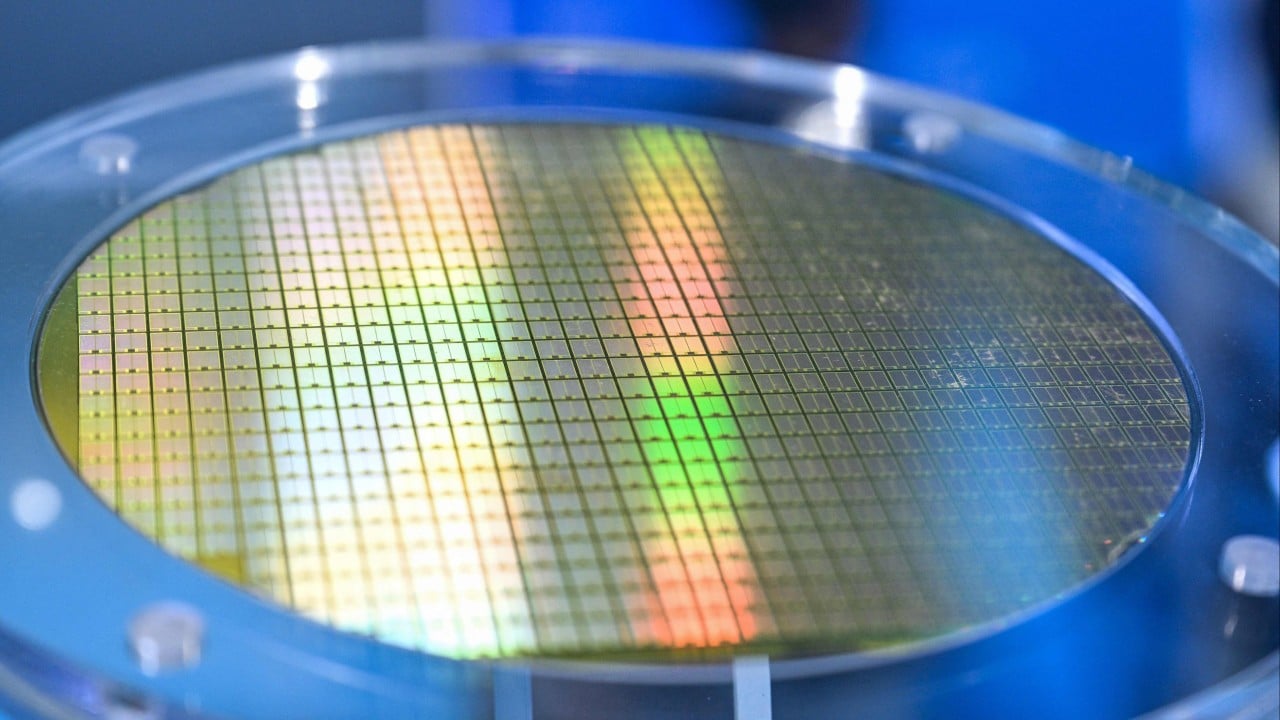
💡A new China-backed bet could open another low-power path for future edge AI chips.
⚡ 30-Second TL;DR
What Changed
A YMTC-backed venture fund has taken a stake in semiconductor manufacturer SOI Micro.
Why It Matters
The investment could accelerate domestic development of low-power chips for edge computing and other constrained-device workloads. For AI hardware teams, a stronger FD-SOI ecosystem may eventually provide another option for efficient inference silicon, although commercial availability and process maturity remain key uncertainties.
What To Do Next
Add FD-SOI to your next edge-inference hardware evaluation and compare its power, performance, and tooling requirements with FinFET alternatives.
Key Points
- •A YMTC-backed venture fund has taken a stake in semiconductor manufacturer SOI Micro.
- •SOI Micro is focused on fully depleted silicon-on-insulator (FD-SOI) chipmaking technology.
- •FD-SOI offers a low-power alternative route that complements conventional semiconductor processes.
- •The investment supports China’s effort to build a more self-reliant domestic chip ecosystem.
🧠 Deep Insight
AI-generated analysis for this event.
🔑 Enhanced Key Takeaways
- •FD-SOI technology is increasingly viewed by Chinese firms as a strategic workaround to US-led export controls on extreme ultraviolet (EUV) lithography equipment, as it can achieve performance gains on more mature process nodes.
- •SOI Micro, also known as Shanghai Simgui Technology, has historically been a key player in the silicon-on-insulator wafer market, providing the foundational substrates necessary for FD-SOI manufacturing.
- •The investment aligns with China's 'Big Fund' (National Integrated Circuit Industry Investment Fund) strategy to localize the entire supply chain, moving beyond memory to specialized logic and analog processes.
- •FD-SOI is particularly well-suited for Internet of Things (IoT) and automotive applications due to its inherent ability to manage power consumption and thermal performance more efficiently than bulk CMOS at similar nodes.
- •YMTC's involvement suggests a diversification strategy, leveraging its capital and manufacturing expertise to foster an ecosystem that reduces reliance on traditional FinFET-based architectures which are harder to produce without advanced lithography.
📊 Competitor Analysis▸ Show
| Feature | FD-SOI (SOI Micro) | FinFET (TSMC/SMIC) | Bulk CMOS (Legacy) |
|---|---|---|---|
| Power Efficiency | High (Excellent for IoT) | Moderate | Low |
| Lithography Needs | Lower (Mature nodes) | High (EUV required) | Low |
| Cost per Die | Lower at 22nm/28nm | Higher | Lowest |
| Primary Use Case | IoT, Automotive, RF | High-Performance Computing | General Purpose |
🛠️ Technical Deep Dive
- FD-SOI utilizes an ultra-thin layer of insulator (Buried Oxide or BOX) placed over the base silicon wafer to reduce parasitic capacitance.
- The technology allows for body biasing, which enables dynamic adjustment of threshold voltage to balance performance and power consumption in real-time.
- Unlike FinFET, which uses a 3D transistor structure, FD-SOI maintains a planar structure, simplifying the manufacturing process and reducing mask counts.
- It offers superior radiation hardness and latch-up immunity, making it highly desirable for aerospace and automotive electronics.
🔮 Future ImplicationsAI analysis grounded in cited sources
⏳ Timeline
Weekly AI Recap
Read this week's curated digest of top AI events →
👉Related Updates

AI-curated news aggregator. All content rights belong to original publishers.
Original source: SCMP Technology ↗