💰钛媒体•Stalecollected in 2h
TSMC: Unshakable AI Industry Dominator
💡TSMC's guidance hike confirms AI chip supply stability — plan your hardware roadmap.
⚡ 30-Second TL;DR
What Changed
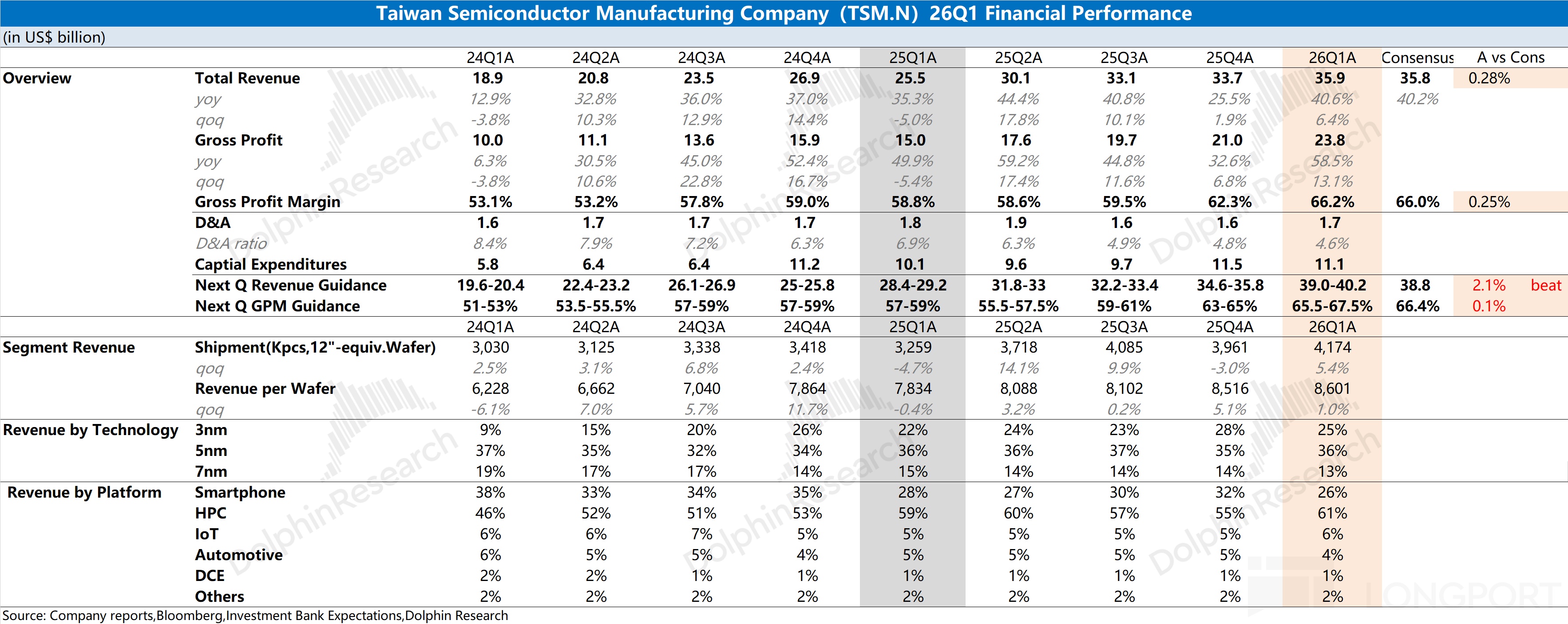
TSMC raises full-year financial guidance
Why It Matters
Signals sustained AI hardware demand growth. Bolsters confidence for AI builders reliant on TSMC fabs. May pressure rivals to innovate faster.
What To Do Next
Assess TSMC's latest node availability for your next AI accelerator design.
Who should care:Enterprise & Security Teams
🧠 Deep Insight
AI-generated analysis for this event.
🔑 Enhanced Key Takeaways
- •TSMC's capital expenditure for 2026 is heavily skewed toward expanding 2nm (N2) process capacity to meet the aggressive demand from hyperscalers for custom AI silicon.
- •The company has successfully transitioned to high-volume manufacturing of its A16 process node, which integrates backside power delivery to improve logic density and power efficiency for next-generation AI accelerators.
- •TSMC is deepening its strategic reliance on CoWoS (Chip-on-Wafer-on-Substrate) advanced packaging, with capacity expansion plans aiming to alleviate the persistent bottleneck in high-bandwidth memory (HBM) integration for AI training clusters.
📊 Competitor Analysis▸ Show
| Feature | TSMC | Samsung Foundry | Intel Foundry |
|---|---|---|---|
| Leading Node | N2 / A16 | SF2 / SF2P | Intel 18A |
| AI Market Share | Dominant (>90% for high-end) | Emerging (Focus on HBM integration) | Challenger (Focus on US-based supply) |
| Packaging | CoWoS / SoIC (Market Leader) | I-Cube / H-Cube | Foveros |
| Pricing Strategy | Premium (High margin) | Aggressive (Volume-driven) | Competitive (Foundry-as-a-Service) |
🛠️ Technical Deep Dive
- •N2 Process Node: Utilizes nanosheet transistor architecture (GAAFET) to achieve significant performance-per-watt gains over FinFET-based N3 nodes.
- •A16 Technology: Introduces Super Power Rail (SPR) backside power delivery, decoupling power and signal routing to reduce IR drop and improve signal integrity in high-performance AI chips.
- •CoWoS-L: Employs local silicon interconnects (LSI) to provide a flexible, high-density interposer solution, enabling the integration of multiple HBM3e stacks with large-die AI processors.
- •SoIC (System-on-Integrated-Chips): Utilizes direct bond copper-to-copper technology for 3D stacking, reducing interconnect pitch and latency compared to traditional micro-bump bonding.
🔮 Future ImplicationsAI analysis grounded in cited sources
TSMC will maintain a greater than 85% market share in the sub-3nm AI chip segment through 2027.
The massive capital investment in N2 and A16 capacity creates a high barrier to entry that competitors cannot match in the short term.
Advanced packaging capacity will become the primary determinant of AI chip revenue growth for TSMC.
As AI chips grow in physical size and memory requirements, the ability to package these components reliably is currently more constrained than wafer fabrication itself.
⏳ Timeline
2022-12
TSMC begins volume production of 3nm (N3) process technology.
2024-04
TSMC announces the A16 process node, featuring backside power delivery.
2025-07
TSMC reports record-breaking demand for CoWoS packaging, leading to accelerated capacity expansion.
2025-12
TSMC achieves initial yield targets for 2nm (N2) process technology.
📰
Weekly AI Recap
Read this week's curated digest of top AI events →
👉Related Updates

AI-curated news aggregator. All content rights belong to original publishers.
Original source: 钛媒体 ↗