🇭🇰SCMP Technology•Stalecollected in 26m
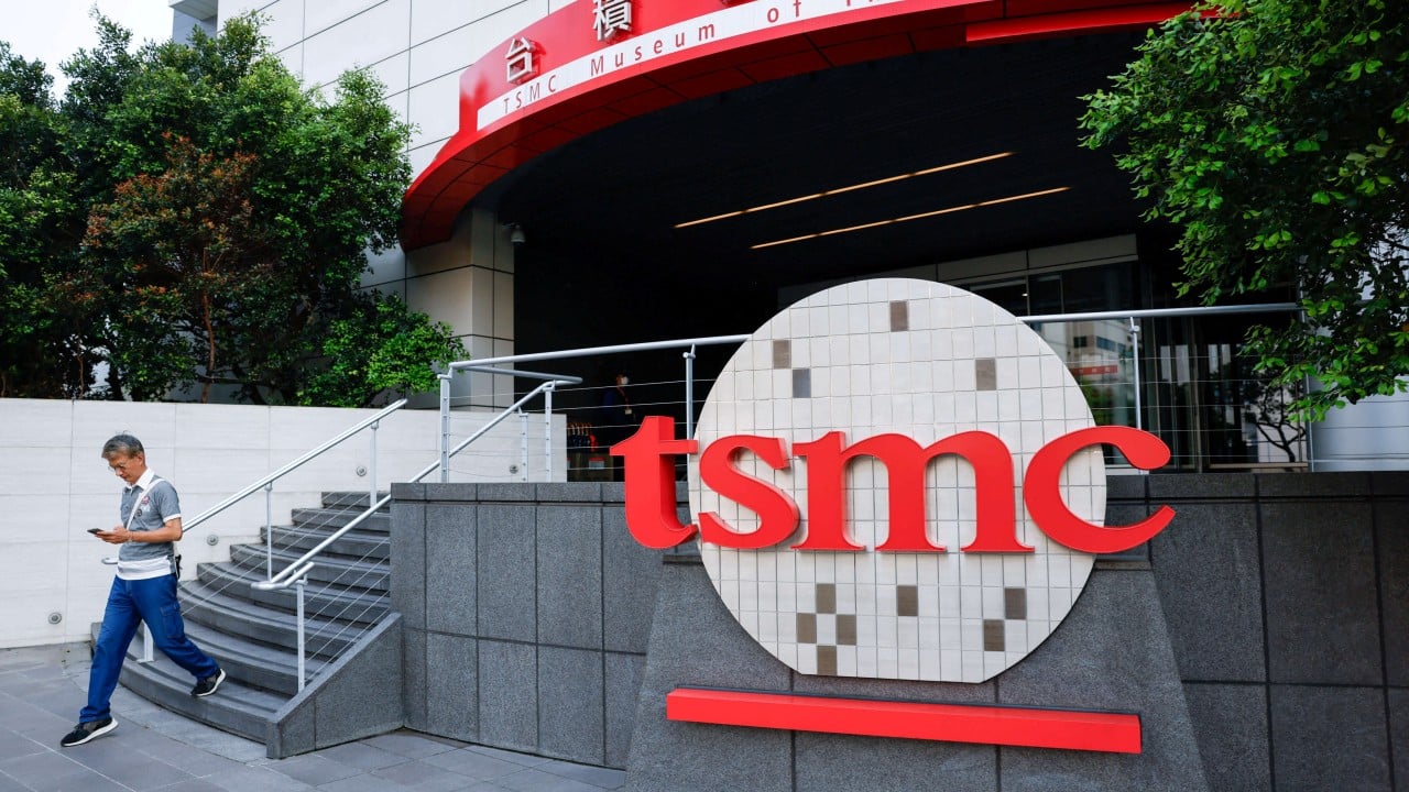
TSMC Targets 30%+ Revenue Surge in 2026 on AI Boom
💡TSMC's 30% revenue jump on AI demand means massive chip supply ramp—vital for AI infra scaling.
⚡ 30-Second TL;DR
What Changed
TSMC expects >30% revenue surge in 2026
Why It Matters
TSMC's expansion signals reliable AI chip supply growth, easing hardware shortages for large-scale deployments. AI firms can anticipate better capacity for training/inference needs, potentially stabilizing costs.
What To Do Next
Assess TSMC supply chain impacts on your Nvidia GPU procurement for 2026 AI projects.
Who should care:Enterprise & Security Teams
🧠 Deep Insight
AI-generated analysis for this event.
🔑 Enhanced Key Takeaways
- •TSMC's 2026 growth trajectory is heavily underpinned by the mass production ramp-up of its A16 (1.6nm) process node, which integrates backside power delivery technology to significantly improve logic density and power efficiency for hyperscale AI accelerators.
- •The company is aggressively expanding its CoWoS (Chip-on-Wafer-on-Substrate) advanced packaging capacity, aiming to alleviate the persistent supply bottlenecks that have constrained AI GPU shipments for major clients like NVIDIA and AMD throughout early 2026.
- •TSMC is diversifying its geographic risk by accelerating the operational timeline of its Arizona 'Fab 21' facilities, which are now slated to contribute meaningful revenue from 4nm and 3nm production volumes by mid-2026.
📊 Competitor Analysis▸ Show
| Feature | TSMC | Samsung Foundry | Intel Foundry |
|---|---|---|---|
| Leading Node | A16 (1.6nm) | SF2 (2nm) | Intel 18A |
| Advanced Packaging | CoWoS (Market Leader) | I-Cube | Foveros |
| AI Market Share | Dominant (High-end) | Growing (Mid-range) | Emerging (Foundry Services) |
🛠️ Technical Deep Dive
- A16 Process Node: Introduces 'Super Power Rail' (backside power delivery) to decouple power and signal routing, reducing IR drop and improving performance by ~8-10% at the same power compared to N2P.
- CoWoS-L/R: Utilization of LSI (Local Silicon Interconnect) and RDL (Redistribution Layer) interposers to enable larger reticle sizes, supporting the integration of multiple HBM3e/HBM4 stacks with high-performance logic dies.
- N2P (2nm Enhanced): Implementation of Gate-All-Around (GAA) nanosheet transistors to provide superior electrostatic control, essential for maintaining performance at sub-2nm scales.
🔮 Future ImplicationsAI analysis grounded in cited sources
TSMC will maintain a >60% global market share in advanced logic nodes through 2026.
The combination of superior yield rates on 3nm/2nm nodes and unmatched capacity in advanced packaging creates a high barrier to entry for competitors.
Capital expenditure will exceed $35 billion for the 2026 fiscal year.
The aggressive ramp-up of A16 production lines and the completion of overseas fabs require sustained, record-level investment.
⏳ Timeline
2022-12
TSMC begins construction of second fab in Arizona, increasing total investment to $40 billion.
2023-08
TSMC announces plans for a joint venture fab in Dresden, Germany, focusing on automotive and industrial chips.
2024-04
TSMC receives $6.6 billion in direct funding from the U.S. CHIPS Act to support domestic manufacturing.
2025-07
TSMC officially initiates volume production of its N2 (2nm) process technology.
2026-01
TSMC reports record-breaking Q4 2025 earnings driven by sustained demand for AI-specific silicon.
📰
Weekly AI Recap
Read this week's curated digest of top AI events →
👉Related Updates


AI-curated news aggregator. All content rights belong to original publishers.
Original source: SCMP Technology ↗