TSMC Targets 1nm with 1 Trillion Transistors
💡TSMC 1nm promises 1T transistors, powering future AI compute density leaps.
⚡ 30-Second TL;DR
What Changed
TSMC holds 70% global foundry market share
Why It Matters
1nm process will enable denser, more efficient chips critical for next-gen AI training and inference, potentially accelerating LLM scaling and reducing power costs for AI infrastructure.
What To Do Next
Track TSMC 1nm timeline via their investor updates for AI chip design planning.
🧠 Deep Insight
Web-grounded analysis with 7 cited sources.
🔑 Enhanced Key Takeaways
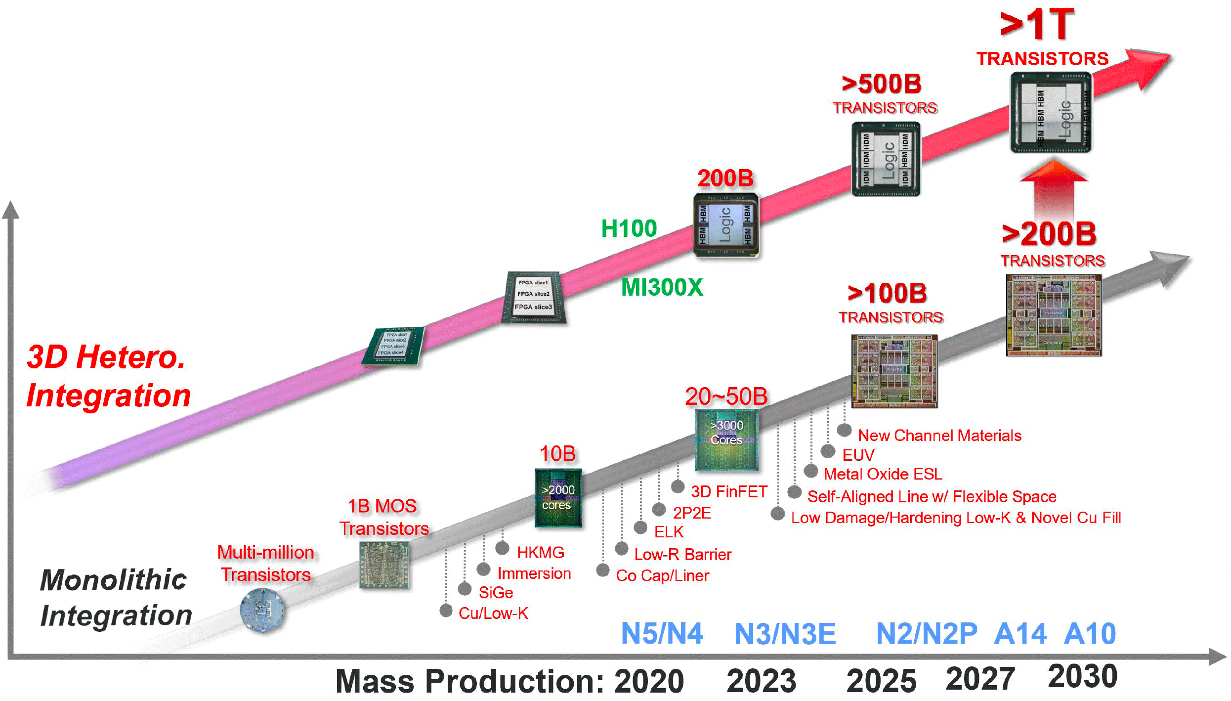
- •TSMC plans 1nm (A10) process for 2030 production, targeting 200 billion transistors per monolithic chip and 1 trillion transistors via 3D packaging with multi-chiplets[1][2].
- •Shalun Science Park will host six fabs: P1-P3 for 1.4nm (A14) and P4-P6 for 1nm, with potential 0.7nm expansion[1].
- •TSMC's A16 (1.6nm) process enters trial production by end-2026 and full production in 2027, featuring backside power delivery for 8-10% speed gains over N2P[1][4].
- •TSMC operates a Hsinchu R&D center with 7,000 researchers developing novel materials and transistor structures like CFET and 2D materials for 1nm[2].
📊 Competitor Analysis▸ Show
| Competitor | Process Node | Target Mass Production | Key Features |
|---|---|---|---|
| Intel | 1.8nm (18A) | 2025 | Backside power |
| Intel | 1.4nm (A14) | 2028 | GAA transistors |
| Samsung | 1.4nm (SF1.4) | 2027 | Yield/cost focus |
| Samsung | 1nm | After 2029 | High-NA EUV |
| Rapidus | 1.4nm | 2027 | IBM/Imec collab |
| Rapidus | 1nm | 2030s | Univ Tokyo/CEA Leti |
🛠️ Technical Deep Dive
- •1nm (A10) rumored to upgrade from GAAFET to CFET (Complementary FET) transistors and integrate 2D materials[1].
- •A16 (1.6nm) uses backside power delivery (BSPDN) for front-side signal routing, improving logic density and performance by 8-10% over N2P, ideal for HPC[4].
- •A14 (1.4nm) incorporates second-generation GAA transistors and backside power delivery[1].
- •TSMC advancing packaging like Chip-on-Wafer-on-Substrate (CoWoS) for 2027 to enable trillion-transistor multi-chiplet systems with HBM integration[2][4].
🔮 Future ImplicationsAI analysis grounded in cited sources
⏳ Timeline
📎 Sources (7)
Factual claims are grounded in the sources below. Forward-looking analysis is AI-generated interpretation.
- smbom.com — 46460
- ednasia.com — TSMC on Track to 1 Nm Node by 2030
- eu.36kr.com — 3441814966441606
- theregister.com — TSMC First 16nm Chips
- design-reuse-embedded.com — Samsung Expected to Unveil Its 1nm Plan in June Advancing It to 2026
- sammyguru.com — Samsung Begins 1nm Process Development Mass Production After 2029
- en.eeworld.com.cn — A406748
Weekly AI Recap
Read this week's curated digest of top AI events →
👉Related Updates


AI-curated news aggregator. All content rights belong to original publishers.
Original source: cnBeta (Full RSS) ↗