📊Bloomberg Technology•Stalecollected in 27m
TSMC-Sony JV Targets Next-Gen Sensors
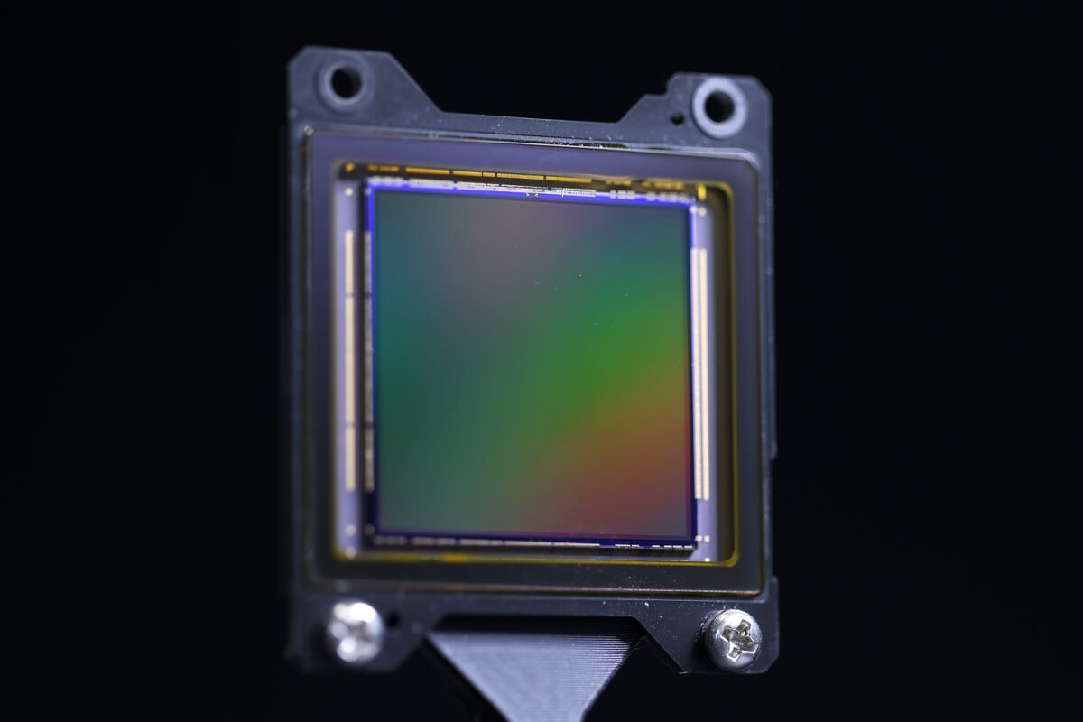
💡TSMC-Sony JV for advanced image sensors: vital for next-gen AI vision hardware
⚡ 30-Second TL;DR
What Changed
TSMC and Sony planning joint venture formation
Why It Matters
Boosts supply of high-performance sensors critical for AI vision systems, potentially lowering costs for computer vision applications in devices.
What To Do Next
Benchmark TSMC-Sony sensors in your CV pipelines for improved image input quality.
Who should care:Developers & AI Engineers
Key Points
- •TSMC and Sony planning joint venture formation
- •Focus on building next-generation image sensors
- •Enhances semiconductor collaboration for sensor tech
🧠 Deep Insight
AI-generated analysis for this event.
🔑 Enhanced Key Takeaways
- •The joint venture, officially known as Japan Advanced Semiconductor Manufacturing (JASM), is located in Kumamoto Prefecture, Japan, and represents a strategic effort to diversify TSMC's manufacturing footprint outside of Taiwan.
- •Sony Semiconductor Solutions holds a minority equity stake in JASM, alongside Denso Corporation, ensuring a dedicated supply chain for high-end CMOS image sensors used in automotive and mobile applications.
- •The facility utilizes TSMC's 12/16nm and 22/28nm process technologies, moving beyond legacy nodes to support the high-performance requirements of next-generation imaging hardware.
📊 Competitor Analysis▸ Show
| Feature | JASM (TSMC/Sony) | Samsung Foundry | Intel Foundry |
|---|---|---|---|
| Primary Focus | CMOS Image Sensors | Integrated Memory/Logic | High-Performance Computing |
| Process Nodes | 12nm - 28nm | 14nm - 3nm | 16nm - 1.8nm |
| Strategic Edge | Dedicated Sony integration | Vertical integration (in-house) | Advanced packaging (Foveros) |
🛠️ Technical Deep Dive
- Utilization of TSMC's N28 and N16 process nodes to optimize power efficiency for high-resolution image signal processing (ISP).
- Integration of Sony's proprietary stacked CMOS sensor architecture, which separates the pixel array from the logic circuit layer.
- Implementation of TSMC's 3D IC packaging technologies to enable higher interconnect density between the sensor and the logic die.
🔮 Future ImplicationsAI analysis grounded in cited sources
JASM will achieve full-scale mass production by late 2026.
The facility has completed equipment installation and is currently in the final stages of yield optimization for its primary sensor product lines.
Sony will reduce its reliance on external foundries for mid-range sensor logic wafers.
The proximity of the JASM facility to Sony's existing Kumamoto sensor fabrication plants significantly lowers logistics costs and cycle times.
⏳ Timeline
2021-11
TSMC and Sony announce the formation of JASM in Kumamoto, Japan.
2022-04
Construction of the JASM fabrication facility officially commences.
2024-02
JASM facility holds its grand opening ceremony with production scheduled to begin.
2025-02
TSMC announces plans for a second fabrication plant in Kumamoto to expand capacity.
📰
Weekly AI Recap
Read this week's curated digest of top AI events →
👉Related Updates
AI-curated news aggregator. All content rights belong to original publishers.
Original source: Bloomberg Technology ↗