🐯虎嗅•Freshcollected in 2m
TSMC Q2 2026 Earnings: AI Growth and Capex Surge
💡Critical insights into AI hardware supply chain bottlenecks and TSMC's aggressive 2nm expansion strategy.
⚡ 30-Second TL;DR
What Changed
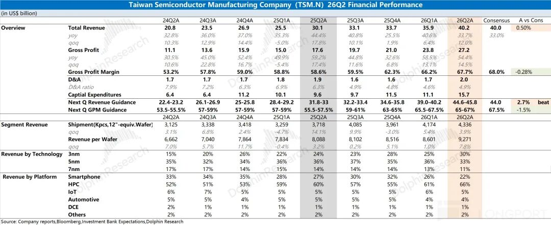
Q2 revenue reached $40.2 billion, with AI-driven HPC accounting for 66% of total income.
Why It Matters
TSMC's increased capex confirms the sustained long-term demand for AI infrastructure, reinforcing its monopoly on advanced packaging and sub-3nm manufacturing.
What To Do Next
Monitor TSMC's CoWoS capacity availability when planning hardware deployment timelines for large-scale AI clusters.
Who should care:Founders & Product Leaders
Key Points
- •Q2 revenue reached $40.2 billion, with AI-driven HPC accounting for 66% of total income.
- •2nm process has officially entered mass production, contributing 3% of quarterly revenue.
- •Annual capital expenditure guidance increased to $60-64 billion, signaling aggressive expansion.
- •CoWoS monthly capacity is expected to reach 120,000 units by the end of 2026.
🧠 Deep Insight
AI-generated analysis for this event.
🔑 Enhanced Key Takeaways
- •TSMC's 2nm (N2) process utilizes Gate-All-Around (GAA) transistor architecture, marking a significant shift from the FinFET technology used in 3nm and earlier nodes.
- •The surge in capital expenditure is heavily allocated toward the construction of 'Giga-fabs' in Arizona and Japan, alongside advanced packaging facilities in Taiwan to alleviate CoWoS bottlenecks.
- •TSMC has secured exclusive manufacturing partnerships for next-generation AI accelerators from major hyperscalers, including custom silicon initiatives from Google, Amazon, and Microsoft.
- •The company reported a record-high gross margin of 58.5% for Q2 2026, attributed to favorable pricing power in the AI sector and improved yield rates for N3E processes.
- •TSMC is accelerating its 'A16' process development, targeting a 2027 production timeline to maintain its lead over competitors by integrating backside power delivery networks.
📊 Competitor Analysis▸ Show
| Feature | TSMC (N2/N3) | Samsung Foundry (SF2/SF3) | Intel Foundry (18A/20A) |
|---|---|---|---|
| Transistor Architecture | GAA (N2) | GAA (SF2) | RibbonFET (18A) |
| AI Market Share | Dominant (>90%) | Emerging | Developing |
| Advanced Packaging | CoWoS (Market Leader) | I-Cube | Foveros |
| Status | Mass Production | Yield Challenges | Ramp-up Phase |
🛠️ Technical Deep Dive
- N2 Process: Implements nanosheet GAA transistors to provide higher drive current and lower power consumption compared to FinFET.
- Backside Power Delivery: TSMC's A16 node will utilize Super Power Rail technology to decouple power and signal routing, reducing IR drop and improving performance.
- CoWoS-R: Utilization of redistribution layers (RDL) interposers to support larger chiplet sizes for high-bandwidth memory (HBM) integration.
- N3E Yield: Optimization of EUV lithography steps has allowed for a 15% improvement in logic density and 30% power reduction over the original N3 node.
🔮 Future ImplicationsAI analysis grounded in cited sources
TSMC will maintain a global foundry market share above 60% through 2027.
The massive capital expenditure in 2nm and advanced packaging creates a high barrier to entry that competitors cannot match in the short term.
AI-driven HPC revenue will exceed 75% of TSMC's total income by Q4 2027.
The continued scaling of large language models and custom AI silicon demand is outpacing the recovery of the consumer electronics and automotive sectors.
⏳ Timeline
2022-12
TSMC begins volume production of 3nm (N3) technology in Tainan.
2024-04
TSMC receives $6.6 billion in CHIPS Act funding for Arizona facility expansion.
2025-02
TSMC officially opens its first specialized manufacturing fab in Kumamoto, Japan.
2026-01
TSMC announces the successful pilot run of 2nm (N2) chips with high yield.
📰
Weekly AI Recap
Read this week's curated digest of top AI events →
👉Related Updates


AI-curated news aggregator. All content rights belong to original publishers.
Original source: 虎嗅 ↗