TSMC Developing CoPoS Packaging Tech for 2028 Launch
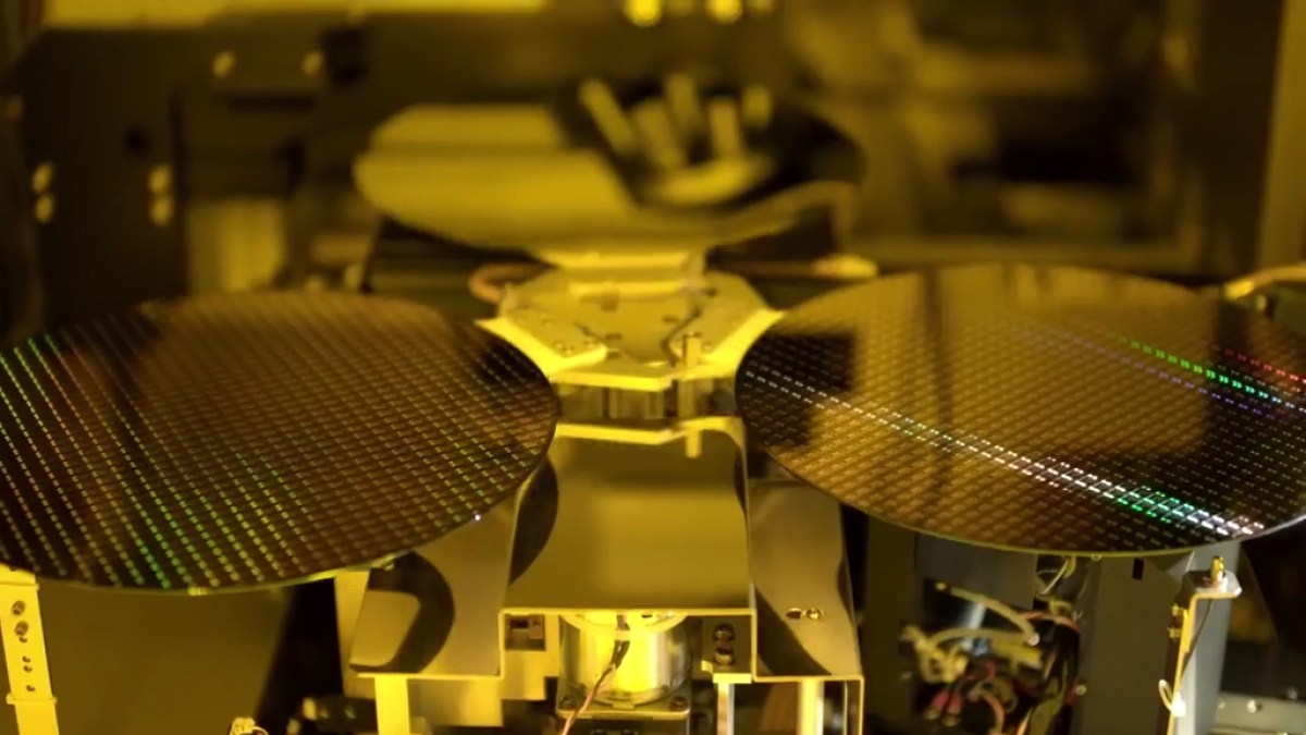
💡New glass-based packaging tech from TSMC could redefine AI chip performance and density by 2028.
⚡ 30-Second TL;DR
What Changed
CoPoS stands for Chip-on-Panel-on-Structure
Why It Matters
This advancement in packaging will likely enhance the thermal and electrical efficiency of future AI accelerators. It represents a critical step in overcoming current limitations in high-performance computing hardware.
What To Do Next
Monitor TSMC's roadmap for glass-substrate integration to plan future hardware procurement for high-compute AI clusters.
Key Points
- •CoPoS stands for Chip-on-Panel-on-Structure
- •Integrates glass material as both a carrier and substrate component
- •Targeting mass production by 2028
- •Features a unique three-layer sandwich design
🧠 Deep Insight
Background and context from public sources — not the original article. 16 sources cited.
🔑 Enhanced Key Takeaways
- •CoPoS represents a panel-level evolution of TSMC's existing CoWoS (Chip-on-Wafer-on-Substrate) technology, transitioning from circular silicon interposers to square glass or organic panels.
- •This shift to rectangular panels significantly boosts substrate utilization from approximately 65% on traditional 12-inch wafers to around 95%, leading to reduced material waste and manufacturing costs, particularly for large AI processors.
- •NVIDIA's Feynman AI chipset is anticipated to be the inaugural adopter of CoPoS, leveraging the expanded panel area to integrate a greater number of High-Bandwidth Memory (HBM) stacks, potentially up to 12 HBM4 chips, alongside multiple GPU chiplets.
- •CoPoS is engineered to circumvent the 'reticle limit' by accommodating panel sizes beyond the constraints of traditional 300mm wafers, with proposed formats including 310x310mm, 510x515mm, and even larger dimensions up to 750x620mm under consideration.
- •The technology is deemed critical for enabling future generations of ultra-large high-performance computing (HPC) and AI chips, and it facilitates the integration of Co-Packaged Optics (CPO) components such as optical engines and couplers.
🛠️ Technical Deep Dive
- CoPoS utilizes glass in two distinct capacities: as temporary carriers measuring 310x310mm during processing, and as glass panels (250x250mm for pilot runs, scaling to 510x515mm for mass production) that are subsequently cut into individual glass core substrates.
- The core substrate features a three-layer sandwich structure, comprising a glass core positioned between Ajinomoto Build-up Film (ABF) layers on both sides, often referred to as ABF-GCP.
- Contrary to some misconceptions, the glass in CoPoS does not function as an interposer. The interconnectivity is managed by the chip-side Redistribution Layer (RDL), complemented by Through-Glass Vias (TGV) and copper interconnects embedded within the glass core substrate stack.
- Both glass and ABF layers coexist within the CoPoS structure; glass does not replace ABF. Chips are directly attached to the ABF build-up surface of the glass core substrate.
- CoPoS is a panel-level packaging (PLP) technology, which is expected to deliver higher throughput and lower cost per unit compared to traditional wafer-level packaging (WLP).
- A significant challenge in the mass production of CoPoS, particularly with expanding substrate sizes, is managing warpage issues.
🔮 Future ImplicationsAI analysis grounded in cited sources
⏳ Timeline
📎 Sources (16)
Factual claims are grounded in the sources below. Forward-looking analysis is AI-generated interpretation.
Weekly AI Recap
Read this week's curated digest of top AI events →
👉Related Updates
AI-curated news aggregator. All content rights belong to original publishers.
Original source: cnBeta (Full RSS) ↗
This is a summary, not the original. Read the source, or get the weekly briefing.
The weekly digest
One email a week. Unsubscribe anytime.