TSMC 3nm Capacity Tight for Non-Loyal Customers
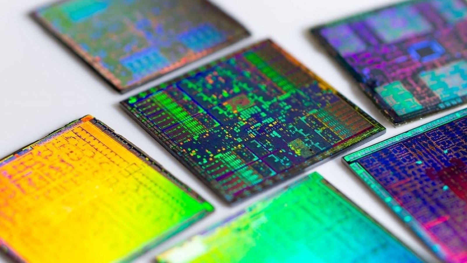
💡TSMC 3nm crunch favors loyalists—scramble for AI chip supply priority.
⚡ 30-Second TL;DR
What Changed
AI boom causes explosive demand for TSMC 3nm process.
Why It Matters
Supply limits disadvantage new entrants in AI hardware, benefiting established players like Nvidia, potentially slowing industry-wide AI chip innovation.
What To Do Next
Assess Samsung or Intel Foundry alternatives if lacking TSMC long-term status for AI chip production.
Key Points
- •AI boom causes explosive demand for TSMC 3nm process.
- •Severe capacity constraints across AI supply chains.
- •Priority allocation only for long-term loyal customers.
- •Insights from Electronic Times industry sources.
🧠 Deep Insight
AI-generated analysis for this event — not the original article.
🔑 Enhanced Key Takeaways
- •TSMC's N3P (3nm enhanced) process node has become the primary driver for high-performance computing (HPC) and AI accelerator demand, leading to a significant shift in wafer allocation strategies toward strategic partners like Apple, NVIDIA, and AMD.
- •The capacity crunch is exacerbated by the transition of major cloud service providers (CSPs) to custom-designed AI silicon, which competes directly with traditional fabless chipmakers for limited 3nm production slots.
- •TSMC has reportedly implemented a 'value-based' pricing model for 3nm capacity, where non-loyal or short-term customers face significant premiums or are deprioritized in favor of long-term capacity reservation agreements.
📊 Competitor Analysis▸ Show
| Feature | TSMC (3nm/N3P) | Samsung Foundry (3nm/SF3) | Intel Foundry (18A) |
|---|---|---|---|
| Maturity | High (Mass Production) | Moderate (Early Production) | Emerging (Ramping) |
| Yield | Industry Leading | Improving | Developing |
| Primary Focus | HPC/AI/Mobile | Mobile/HPC | HPC/Internal/Foundry |
🛠️ Technical Deep Dive
- •TSMC 3nm family utilizes FinFlex technology, allowing designers to mix and match standard cells within the same block to optimize for power, performance, and area (PPA).
- •N3P process node offers approximately 5% speed improvement, 5-10% power reduction, and 1.04x density improvement compared to the base N3E node.
- •The process employs extreme ultraviolet (EUV) lithography with high-NA EUV tools being integrated into subsequent iterations to manage complex patterning requirements for sub-3nm features.
🔮 Future ImplicationsAI analysis grounded in cited sources
⏳ Timeline
Weekly AI Recap
Read this week's curated digest of top AI events →
👉Related Updates
AI-curated news aggregator. All content rights belong to original publishers.
Original source: cnBeta (Full RSS) ↗
This is a summary, not the original. Read the source, or get the weekly briefing.
The weekly digest
One email a week. Unsubscribe anytime.