The Race to Commercialize Glass Core Substrates in Packaging
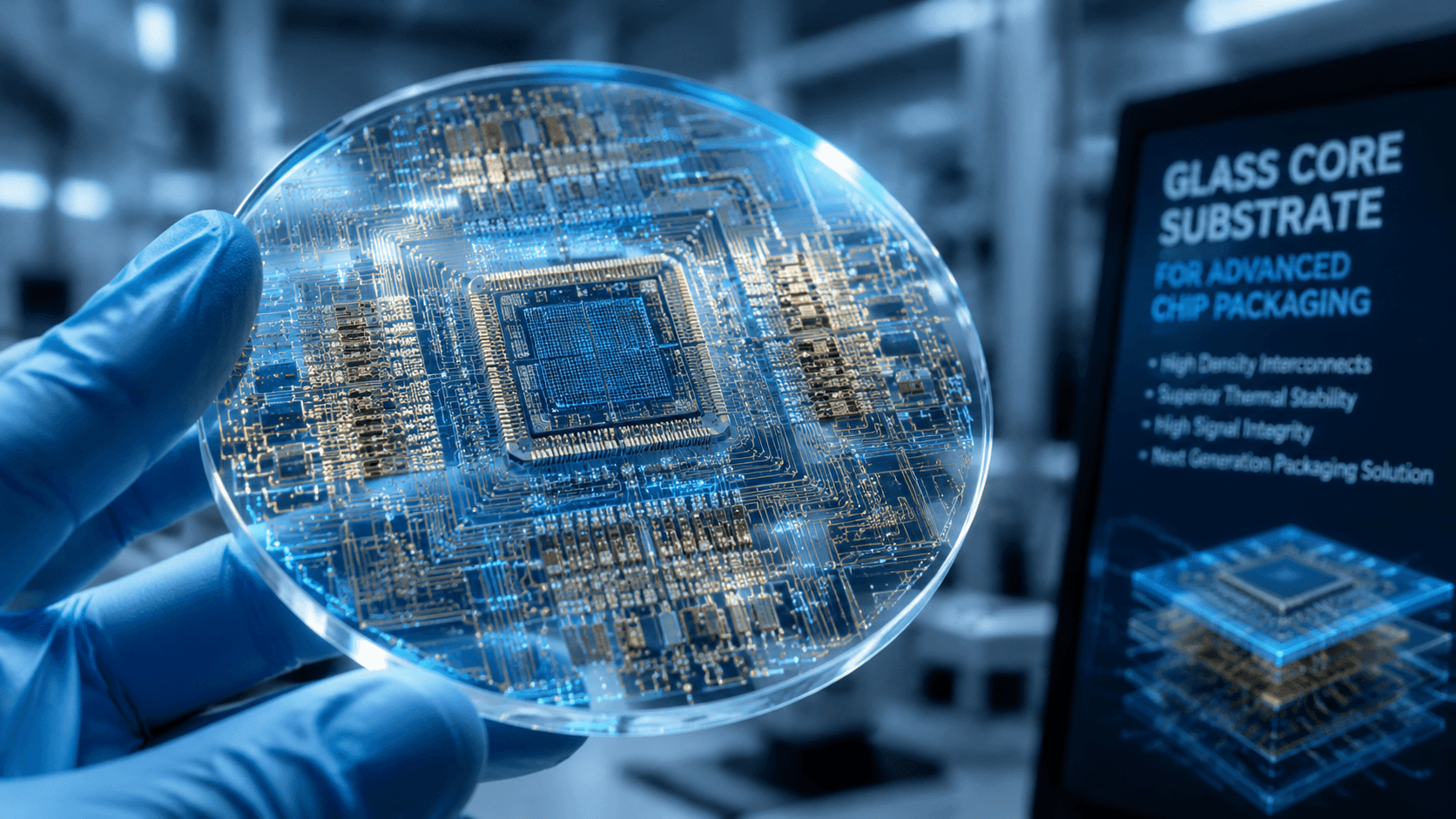
💡Glass substrates are the next frontier for AI hardware, potentially solving thermal limits in high-end GPUs.
⚡ 30-Second TL;DR
What Changed
Glass substrates offer superior electrical and thermal properties over organic substrates
Why It Matters
Successful commercialization of glass substrates could significantly alleviate thermal bottlenecks in high-density AI GPU clusters.
What To Do Next
Monitor the supply chain roadmaps of major semiconductor foundries regarding glass substrate integration for next-gen AI hardware.
Key Points
- •Glass substrates offer superior electrical and thermal properties over organic substrates
- •Industry debate persists regarding the timeline for true mass-market adoption
- •Critical technology for high-performance AI chip packaging
🧠 Deep Insight
Background and context from public sources — not the original article. 25 sources cited.
🔑 Enhanced Key Takeaways
- •Intel has been a significant driver in the development of glass core substrates, committing to the technology in its advanced packaging roadmap as early as 2023 and showcasing initial prototypes in early 2026.
- •Glass core substrates enable significantly higher interconnect density, potentially up to 10 times, and finer redistribution layer (RDL) features, pushing below the 2-micrometer line/space limit of organic substrates.
- •The inherent transparency of glass facilitates the integration of co-packaged optics (CPO) and embedded waveguides, which is crucial for dramatically reducing latency and power consumption in data centers and AI systems.
- •Despite their advantages, mass production of glass core substrates faces significant challenges, including the material's brittleness, the complexity of reliably fabricating through-glass vias (TGVs) at scale, and the need for advanced inspection systems to detect microscopic cracks.
- •The market for glass core substrates is projected for substantial growth, with a Compound Annual Growth Rate (CAGR) of 67.2% from 2028 to 2040, potentially becoming a $13 billion opportunity by 2040.
📊 Competitor Analysis▸ Show
| Feature/Property | Glass Core Substrates | Organic Substrates (e.g., ABF) | Silicon Interposers |
|---|---|---|---|
| Warpage | Significantly lower (up to 50% less), ultra-flat. | Higher, increasing with package size. | Higher than glass, 50% more warpage than glass. |
| CTE Match to Silicon | Tailorable (3-10 ppm/°C), closely matches silicon (2.6 ppm/°C). | Higher (approx. 7-17 ppm/°C), significant mismatch. | Good match to silicon. |
| Interconnect Density | Enables <2µm line/space RDLs, up to 10x higher density. | Struggles to achieve <2µm line/space. | Very fine wiring, but limited panel size. |
| Dielectric Constant (Dk) | Low (2.5-6 at 10 GHz), significantly lower than silicon. | Moderate (3.5-4.5 for FR-4, ~7 for OCS). | High (12). |
| Dissipation Factor (Df) | Very low (0.0005-0.005 at 10 GHz). | Higher (0.015-0.025 for FR-4). | Higher than glass. |
| Panel Size | Can be fabricated in large panels (e.g., 700x700mm, 510x515mm). | Limited by warpage issues at larger sizes. | Limited to wafer sizes, smaller than glass panels. |
| Cost | Potentially lower per-unit cost with large panels, but high initial investment. | Generally cost-effective for mainstream. | More expensive than glass. |
| Brittleness | Inherently brittle, prone to microcracks. | Flexible, less brittle. | Brittle. |
| Thermal Conductivity | 1.0–1.4 W/(m·K), comparable to high-performance organics. | 0.3–0.8 W/(m·K) for FR-4, 1.0–2.0 W/(m·K) for high-performance organics. | |
| Optical Transparency | Transparent, enables co-packaged optics. | Opaque. | Opaque. |
🛠️ Technical Deep Dive
- Material Composition: Typically inorganic silicate glass matrix, such as borosilicate or aluminosilicate, containing 60–70 wt% SiO₂, 10–15 wt% B₂O₃, and 5–10 wt% Al₂O₃.
- Thickness: Glass core substrates range in thickness from 50 μm to 500 μm, with ultrathin glass capable of being less than 100 μm.
- Coefficient of Thermal Expansion (CTE): Can be precisely tailored from 3 to 10 ppm/°C, allowing for a close match with silicon (2.6 ppm/°C) to minimize thermomechanical stress.
- Dielectric Constant (Dk): Borosilicate glass cores exhibit Dk values between 4.6 and 6.2 at 1 GHz, and as low as 2.5-6 at 10 GHz, significantly lower than silicon (12) and organic laminates (3.5-4.5 for FR-4).
- Dissipation Factor (Df): Values typically range from 0.003–008 at 1 GHz, and as low as 0.0005-0.005 at 10 GHz, which is considerably lower than organic substrates (0.015–0.025 for standard FR-4).
- Thermal Conductivity: Glass core substrates generally have a thermal conductivity of 1.0–1.4 W/(m·K).
- Through-Glass Vias (TGVs): These provide vertical electrical paths, with typical resistance values of 5–20 mΩ for 50 μm diameter, 100 μm length vias filled with electroplated copper. Via-to-via capacitance is 0.05–0.15 pF for 50 μm diameter vias with 100 μm pitch.
- Redistribution Layers (RDLs): Glass substrates enable the creation of fine-pitch RDLs with line and space features below 2 μm.
- Manufacturing Processes: Involves precision micromachining for TGV formation, metallization (e.g., full copper fill or sidewall plating), and patterning of build-up layers using semi-additive processes. Wet etching can be used to form precisely dimensioned cavities in multi-layered glass.
- Panel Sizes: Glass can be manufactured in large panel formats, such as 700 x 700mm, 510 x 515mm, or 600 x 600mm, which is advantageous for panel-level packaging.
🔮 Future ImplicationsAI analysis grounded in cited sources
⏳ Timeline
📎 Sources (25)
Factual claims are grounded in the sources below. Forward-looking analysis is AI-generated interpretation.
- trendforce.com
- intel.com
- semiengineering.com
- medium.com
- ipcb.com
- ats.net
- chiplet-marketplace.com
- wccftech.com
- economy.ac
- tomshardware.com
- semi.org
- semi.org
- pcdandf.com
- researchgate.net
- patsnap.com
- idtechex.com
- semitracks.com
- pcbmake.com
- corning.com
- a2globalelectronics.com
- medium.com
- neg.co.jp
- corning.com
- imapsource.org
- patsnap.com
Weekly AI Recap
Read this week's curated digest of top AI events →
👉Related Updates

AI-curated news aggregator. All content rights belong to original publishers.
Original source: Pandaily ↗
This is a summary, not the original. Read the source, or get the weekly briefing.
The weekly digest
One email a week. Unsubscribe anytime.