🇭🇰SCMP Technology•Stalecollected in 31m
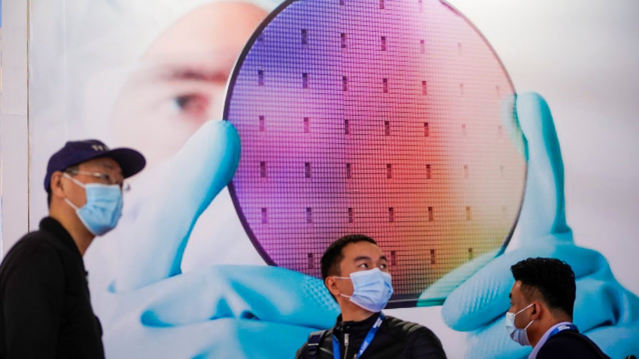
SMIC Launches 2026 Growth Action Plan
💡SMIC's plan accelerates China's chip self-sufficiency, key for AI infra amid trade tensions.
⚡ 30-Second TL;DR
What Changed
SMIC launches action plan targeting 2026 for business enhancement
Why It Matters
SMIC's strategy could boost China's advanced node production, easing AI chip supply constraints amid US export curbs. This may enable more affordable domestic AI hardware for practitioners, diversifying global supply chains.
What To Do Next
Assess SMIC's node advancements for diversifying AI chip suppliers beyond TSMC.
Who should care:Enterprise & Security Teams
Key Points
- •SMIC launches action plan targeting 2026 for business enhancement
- •Released alongside 2025 annual report in stock exchange filing
- •Focuses on optimizing existing operations and new growth increments
- •Positions SMIC as core to China's chip self-sufficiency efforts
🧠 Deep Insight
AI-generated analysis for this event.
🔑 Enhanced Key Takeaways
- •SMIC's 2026 plan explicitly prioritizes the expansion of mature-node capacity (28nm and above) to meet surging domestic demand for IoT, automotive, and industrial chips, despite ongoing US-led export restrictions on advanced lithography equipment.
- •The strategy includes a significant increase in R&D expenditure aimed at improving yield rates for 7nm and 5nm-class processes using existing DUV (Deep Ultraviolet) lithography tools through multi-patterning techniques.
- •The company is shifting its capital expenditure focus toward domestic supply chain integration, aiming to increase the percentage of locally sourced semiconductor equipment and materials to mitigate geopolitical supply chain risks.
📊 Competitor Analysis▸ Show
| Feature | SMIC | TSMC | Samsung Foundry |
|---|---|---|---|
| Primary Focus | Mature nodes / Domestic supply | Advanced nodes / Global supply | Advanced nodes / Memory integration |
| Lithography | DUV (Multi-patterning) | EUV / High-NA EUV | EUV / High-NA EUV |
| Market Position | China self-sufficiency leader | Global market leader | Global technology challenger |
🛠️ Technical Deep Dive
- •Utilization of multi-patterning (SAQP/SADP) on DUV immersion lithography systems to achieve sub-10nm feature sizes.
- •Implementation of advanced packaging technologies, including 2.5D chip-on-wafer-on-substrate (CoWoS) equivalents, to enhance performance for AI-related chipsets.
- •Development of proprietary FinFET process optimization to improve power efficiency and thermal management for high-performance computing (HPC) applications.
- •Integration of domestic EDA (Electronic Design Automation) software tools into the design-to-manufacturing workflow to reduce reliance on Western software suites.
🔮 Future ImplicationsAI analysis grounded in cited sources
SMIC will achieve a 30% increase in domestic equipment utilization by end-of-year 2026.
The company's strategic pivot toward local supply chain integration is a direct response to tightening international export controls on semiconductor manufacturing equipment.
SMIC's profitability will face short-term pressure due to high R&D costs for advanced node yield improvements.
The reliance on multi-patterning techniques with DUV tools significantly increases manufacturing complexity and cost per wafer compared to standard EUV processes.
⏳ Timeline
2020-12
SMIC added to the US Department of Commerce Entity List, restricting access to advanced US technology.
2022-07
Reports emerge of SMIC successfully shipping 7nm-class chips using DUV lithography.
2023-09
SMIC plays a critical role in the manufacturing of the Kirin 9000s processor for Huawei's Mate 60 series.
2025-03
SMIC releases 2024 annual report highlighting record revenue despite geopolitical headwinds.
2026-03
SMIC releases 2025 annual report and officially unveils the 2026 Growth Action Plan.
📰
Weekly AI Recap
Read this week's curated digest of top AI events →
👉Related Updates
AI-curated news aggregator. All content rights belong to original publishers.
Original source: SCMP Technology ↗