🇨🇳cnBeta (Full RSS)•Stalecollected in 19h
SK Hynix Splurges on EUV for Memory Surge
💡SK Hynix EUV buy ramps memory for AI data centers, easing supply crunch.
⚡ 30-Second TL;DR
What Changed
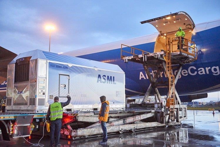
SK Hynix allocates 119.5 trillion KRW for ASML EUV purchase
Why It Matters
Boosts memory supply critical for AI GPUs and data centers, potentially easing HBM shortages for Nvidia Blackwell training. Stabilizes costs for AI infrastructure scaling.
What To Do Next
Track SK Hynix Q2 earnings for HBM production timelines affecting AI GPU availability.
Who should care:Enterprise & Security Teams
🧠 Deep Insight
AI-generated analysis for this event.
🔑 Enhanced Key Takeaways
- •The 119.5 trillion KRW investment is part of a broader multi-year strategic roadmap focused on the Yongin Semiconductor Cluster, designed to secure long-term production capacity for HBM (High Bandwidth Memory) and next-generation DRAM.
- •SK Hynix's aggressive adoption of EUV lithography is specifically targeted at overcoming the physical scaling limitations of sub-10nm DRAM processes, which are essential for meeting the power and density requirements of AI-centric data centers.
- •The capital expenditure shift reflects a strategic pivot to prioritize high-margin HBM production over legacy commodity DRAM, aiming to insulate the company from the historical volatility of the memory market cycle.
📊 Competitor Analysis▸ Show
| Feature | SK Hynix | Samsung Electronics | Micron Technology |
|---|---|---|---|
| EUV Adoption Strategy | Aggressive, focused on HBM/DRAM scaling | Incremental, balancing legacy and advanced nodes | Conservative, prioritizing multi-patterning before EUV |
| Primary Market Focus | AI-optimized HBM3E/HBM4 | Diversified (Mobile, Server, HBM) | Data Center & Edge AI |
| Production Capacity | Rapidly expanding via Yongin Cluster | Massive, utilizing Pyeongtaek facilities | Focused on US/Japan expansion |
🛠️ Technical Deep Dive
- EUV (Extreme Ultraviolet) Lithography: Utilizes 13.5nm wavelength light to enable single-patterning for critical layers in DRAM, replacing complex multi-patterning DUV (Deep Ultraviolet) processes.
- HBM Integration: EUV is critical for the fabrication of high-density DRAM dies used in HBM stacks, allowing for smaller cell sizes and improved signal integrity.
- Process Node: The investment supports the transition to 1b and 1c nanometer-class DRAM nodes, which are essential for achieving the density required for 32Gb+ density chips.
🔮 Future ImplicationsAI analysis grounded in cited sources
SK Hynix will achieve a dominant market share in the HBM sector by 2027.
Early and aggressive investment in EUV-enabled capacity allows the company to meet the specific technical requirements of major AI chip designers faster than competitors.
Memory industry capital expenditure will shift permanently toward EUV-based manufacturing.
The physical limitations of DUV lithography at advanced nodes make EUV the only viable path for scaling DRAM density to meet AI demand.
⏳ Timeline
2021-07
SK Hynix receives its first EUV lithography machine from ASML for DRAM production.
2023-04
SK Hynix announces the mass production of its 1a nanometer DRAM using EUV technology.
2024-03
SK Hynix begins mass production of HBM3E, leveraging advanced lithography techniques.
2025-06
SK Hynix breaks ground on the first phase of the Yongin Semiconductor Cluster to house new EUV-equipped fabs.
📰
Weekly AI Recap
Read this week's curated digest of top AI events →
👉Related Updates
AI-curated news aggregator. All content rights belong to original publishers.
Original source: cnBeta (Full RSS) ↗