💰钛媒体•Stalecollected in 17m
Semicon Giants Enter Hybrid Bonding for HBM
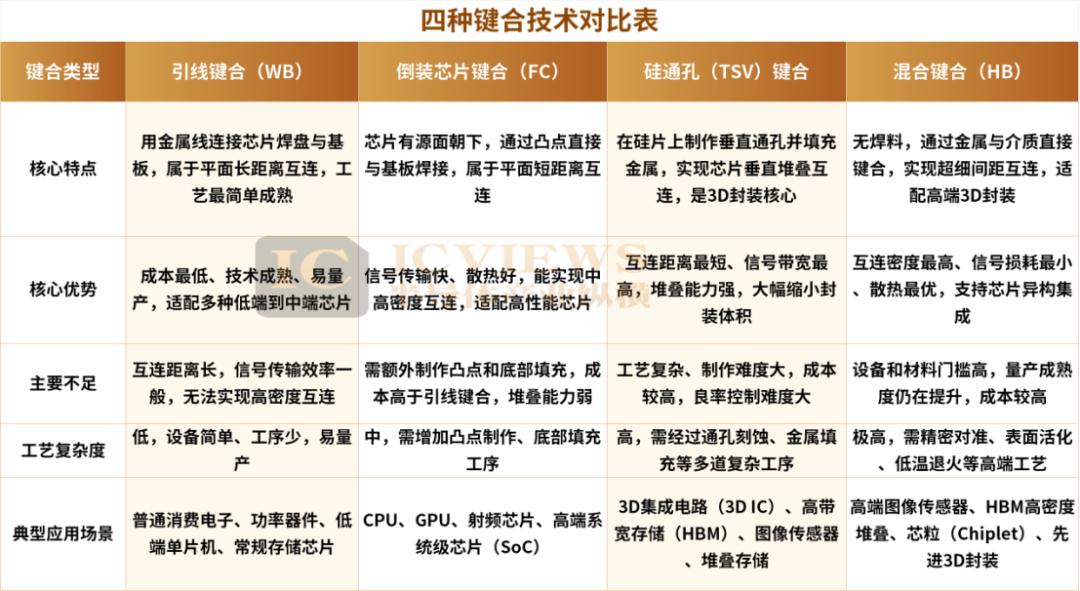
💡Semicon leaders' hybrid bonding push signals faster HBM for AI GPUs
⚡ 30-Second TL;DR
What Changed
Storage leaders entering hybrid bonding field
Why It Matters
Accelerates HBM evolution for denser, faster AI memory stacks. Benefits Nvidia-like GPU makers and AI data centers with superior bandwidth.
What To Do Next
Assess hybrid bonding HBM prototypes from foundry partners like TSMC for AI accelerator designs.
Who should care:Enterprise & Security Teams
Key Points
- •Storage leaders entering hybrid bonding field
- •Foundry giants investing in HBM-compatible tech
- •Equipment makers accelerating hybrid bonding adoption
- •HBM with hybrid bonding imminent
🧠 Deep Insight
AI-generated analysis for this event.
🔑 Enhanced Key Takeaways
- •Hybrid bonding is transitioning from R&D to high-volume manufacturing (HVM) to overcome the pitch limitations of traditional micro-bumps, which are struggling to scale below 20-30 micrometers for next-generation HBM stacks.
- •The adoption of copper-to-copper (Cu-to-Cu) direct bonding is critical for achieving the vertical interconnect density required for HBM4 and beyond, enabling higher bandwidth and lower power consumption per bit.
- •Major equipment suppliers are focusing on wafer-to-wafer (W2W) and die-to-wafer (D2W) bonding alignment accuracy, with sub-micron precision now being the primary competitive differentiator for tool manufacturers.
📊 Competitor Analysis▸ Show
| Feature | Hybrid Bonding (Cu-to-Cu) | Traditional Micro-bumps | Solder-based TSV |
|---|---|---|---|
| Interconnect Pitch | < 10 µm | 20 - 50 µm | > 50 µm |
| Bandwidth Density | Ultra-High | Moderate | Low |
| Thermal Resistance | Low (Direct Metal Path) | High (Underfill/Solder) | High |
| Manufacturing Complexity | Very High | Moderate | Low |
🛠️ Technical Deep Dive
- Cu-to-Cu Bonding Mechanism: Utilizes surface activation and thermocompression to create a direct metallic bond without solder, eliminating the need for underfill and reducing interconnect height.
- Alignment Precision: Requires advanced lithography-grade alignment tools capable of < 0.5 µm overlay accuracy to ensure proper contact between copper pads.
- Surface Preparation: Employs Chemical Mechanical Planarization (CMP) to achieve extreme surface flatness (nanometer-scale roughness) to ensure void-free bonding interfaces.
- HBM Integration: Enables the stacking of more DRAM dies within the same Z-height constraint by removing the bulky micro-bump and underfill layers.
🔮 Future ImplicationsAI analysis grounded in cited sources
HBM4 will exclusively utilize hybrid bonding for high-density vertical stacking.
Traditional micro-bump technology cannot meet the bandwidth and power efficiency requirements mandated by the next generation of AI accelerators.
Hybrid bonding will significantly increase the cost of HBM production in the short term.
The requirement for ultra-precise alignment tools and stringent cleanroom processes for surface preparation increases manufacturing cycle times and yield risks.
⏳ Timeline
2023-09
Industry leaders announce roadmap shifts toward hybrid bonding for HBM4 to address bandwidth bottlenecks.
2024-05
Major semiconductor equipment manufacturers begin shipping pilot-line hybrid bonding tools to memory vendors.
2025-11
Initial successful qualification of hybrid-bonded HBM prototypes reported by leading memory manufacturers.
📰
Weekly AI Recap
Read this week's curated digest of top AI events →
👉Related Updates

AI-curated news aggregator. All content rights belong to original publishers.
Original source: 钛媒体 ↗