🇨🇳cnBeta (Full RSS)•Freshcollected in 4h
Samsung Wins Anthropic 2nm AI Chip Contract
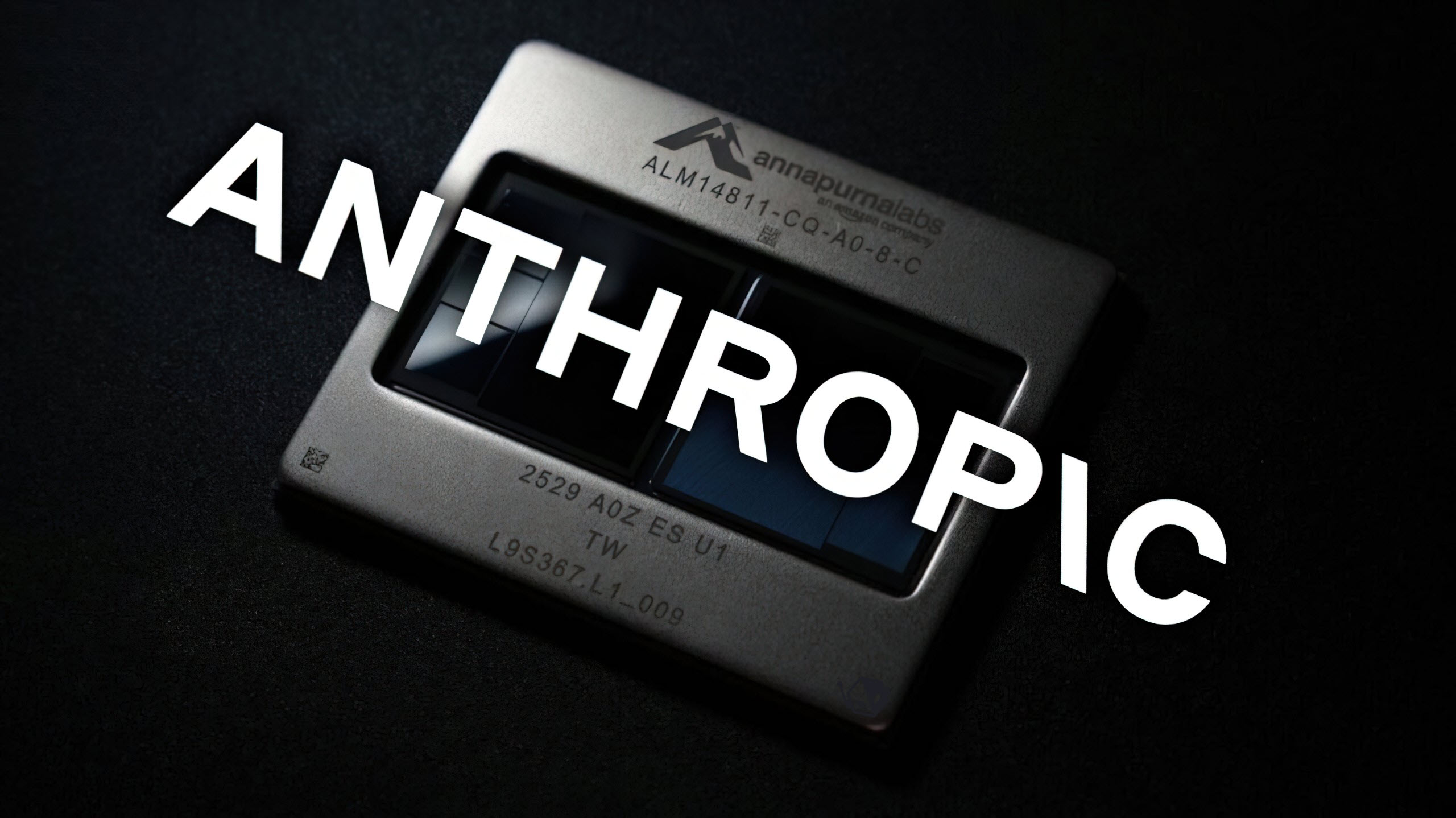
💡Anthropic joins the custom silicon race, choosing Samsung's 2nm process to power its next-gen AI models.
⚡ 30-Second TL;DR
What Changed
Samsung Foundry will manufacture custom AI chips for Anthropic using 2nm technology.
Why It Matters
Anthropic's move to custom silicon suggests a trend of AI labs seeking vertical integration to optimize performance and reduce dependency on standard GPUs.
What To Do Next
Evaluate the potential of custom silicon for your AI model deployment if you are scaling beyond standard cloud GPU instances.
Who should care:Founders & Product Leaders
Key Points
- •Samsung Foundry will manufacture custom AI chips for Anthropic using 2nm technology.
- •The deal aims to help Samsung Foundry return to growth and improve financial performance.
- •Samsung is also advancing the tape-out process for Tesla's AI5 chip.
🧠 Deep Insight
AI-generated analysis for this event.
🔑 Enhanced Key Takeaways
- •The partnership leverages Samsung's Gate-All-Around (GAA) transistor architecture, which is critical for the power efficiency required by Anthropic's large-scale AI models.
- •This deal marks a significant shift for Anthropic, which has historically relied heavily on TSMC for its hardware requirements, signaling a diversification strategy to mitigate supply chain risks.
- •Samsung's 2nm process (SF2) is reportedly being optimized for high-bandwidth memory (HBM) integration, a key requirement for Anthropic's next-generation inference chips.
- •Industry analysts suggest the contract includes a 'co-design' component where Anthropic engineers work directly with Samsung's design services team to optimize chip architecture for Claude model workloads.
- •The agreement is part of a broader South Korean government initiative to foster domestic semiconductor partnerships, providing Samsung with additional subsidies for R&D related to this specific production line.
📊 Competitor Analysis▸ Show
| Feature | Samsung (SF2) | TSMC (N2) | Intel (18A) |
|---|---|---|---|
| Transistor Architecture | GAA (MBCFET) | FinFET (N2) / GAA (N2P) | RibbonFET (GAA) |
| Maturity Status | Early Production | Early Production | Risk Production |
| Primary Advantage | Power Efficiency | Ecosystem/Yield | Backside Power Delivery |
| Target Market | AI Accelerators | High-Performance Computing | General Purpose/AI |
🛠️ Technical Deep Dive
- Samsung's 2nm process utilizes Multi-Bridge-Channel FET (MBCFET) technology, which allows for greater current control compared to traditional FinFET designs.
- The process node is designed to support 2.5D and 3D advanced packaging solutions, essential for integrating HBM3e or HBM4 memory stacks directly with the AI compute die.
- Implementation focuses on reducing parasitic capacitance, which is vital for the high-frequency switching required by Anthropic's transformer-based model architectures.
- The design flow incorporates Samsung's proprietary 'Advanced Foundry Ecosystem' (SAFE) tools, specifically tuned for AI-centric chip layouts.
🔮 Future ImplicationsAI analysis grounded in cited sources
Samsung Foundry will achieve a double-digit increase in its global foundry market share by Q4 2027.
Securing a major hyperscaler-adjacent client like Anthropic provides the volume and technical validation necessary to attract other tier-one AI chip designers.
Anthropic will reduce its reliance on TSMC for primary AI chip production to below 70% by 2028.
The successful integration of Samsung's 2nm process into their hardware roadmap creates a viable dual-sourcing strategy that reduces dependency on a single foundry.
⏳ Timeline
2022-06
Samsung begins mass production of 3nm chips using GAA technology.
2024-06
Samsung Foundry Forum 2024 unveils the roadmap for SF2 (2nm) process technology.
2025-03
Samsung announces successful tape-out of initial test chips on the 2nm process node.
2026-02
Samsung and Tesla reach a milestone in the AI5 chip development process.
📰
Weekly AI Recap
Read this week's curated digest of top AI events →
👉Related Updates


AI-curated news aggregator. All content rights belong to original publishers.
Original source: cnBeta (Full RSS) ↗