📊Bloomberg Technology•Stalecollected in 13m
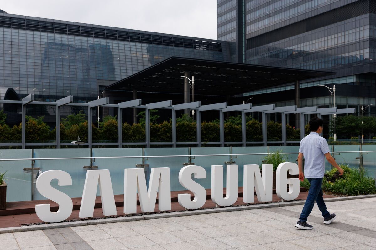
Samsung Profit Soars 8x on AI Chips
💡AI memory demand defies wars—key for scaling your GPU infrastructure
⚡ 30-Second TL;DR
What Changed
Quarterly profit jumped eight-fold due to AI memory chip sales
Why It Matters
Signals sustained AI infrastructure demand, easing supply concerns for practitioners scaling models. Samsung's strength bolsters global chip availability despite geopolitics.
What To Do Next
Assess Samsung HBM3E availability for your next AI training cluster procurement.
Who should care:Enterprise & Security Teams
Key Points
- •Quarterly profit jumped eight-fold due to AI memory chip sales
- •Demand robust for chips in AI and data centers
- •Results exceeded expectations amid Middle East war fears
🧠 Deep Insight
AI-generated analysis for this event.
🔑 Enhanced Key Takeaways
- •Samsung's HBM3E and HBM4 production capacity has been significantly expanded at the Pyeongtaek P4 facility to meet hyperscaler demand for generative AI training clusters.
- •The profit surge was bolstered by a recovery in NAND flash pricing, which saw a 15% sequential increase due to high-density storage requirements for AI server deployments.
- •Samsung successfully transitioned to 1b-nanometer process technology for its latest DRAM offerings, improving power efficiency by 20% compared to previous generations.
📊 Competitor Analysis▸ Show
| Feature | Samsung Electronics | SK Hynix | Micron Technology |
|---|---|---|---|
| HBM Market Position | Strong (Scaling HBM4) | Market Leader (HBM3E) | Challenger (HBM3E) |
| Process Node | 1b-nm DRAM | 1b-nm DRAM | 1-gamma nm DRAM |
| Primary AI Focus | Turnkey AI Solutions | High-Bandwidth Memory | High-Capacity Enterprise SSDs |
🛠️ Technical Deep Dive
- Implementation of 12-layer and 16-layer HBM3E stacks utilizing Advanced Thermal Compression Non-Conductive Film (TC-NCF) technology to manage heat dissipation.
- Integration of TSV (Through-Silicon Via) technology with a 30% reduction in chip-to-chip vertical interconnect pitch to enhance data transfer speeds.
- Adoption of EUV (Extreme Ultraviolet) lithography for critical layers in 1b-nm DRAM to achieve higher bit density and lower power consumption per gigabit.
🔮 Future ImplicationsAI analysis grounded in cited sources
Samsung will increase capital expenditure for foundry services by at least 15% in Q3 2026.
The company needs to accelerate its 2nm GAA (Gate-All-Around) process node deployment to compete with TSMC for next-generation AI accelerator contracts.
Average Selling Prices (ASP) for enterprise-grade NAND will remain elevated through the end of 2026.
Persistent supply constraints for high-capacity QLC NAND, driven by AI data center storage requirements, will continue to support pricing power.
⏳ Timeline
2024-02
Samsung announces development of industry-first 36GB HBM3E 12-layer stack.
2024-11
Samsung initiates mass production of 1b-nm DRAM for AI applications.
2025-06
Samsung expands Pyeongtaek P4 facility to prioritize high-bandwidth memory production.
2026-01
Samsung reports initial yield improvements for HBM4 pilot production lines.
📰
Weekly AI Recap
Read this week's curated digest of top AI events →
👉Related Updates
AI-curated news aggregator. All content rights belong to original publishers.
Original source: Bloomberg Technology ↗