📊Bloomberg Technology•Freshcollected in 26m
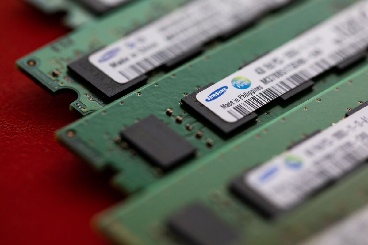
Samsung Hits $1T Valuation on AI Chip Boom
💡Samsung's $1T valuation shows AI memory boom—vital for training cost forecasts
⚡ 30-Second TL;DR
What Changed
Samsung achieves $1T market cap
Why It Matters
Highlights explosive growth in AI infrastructure demand, signaling stable memory supply for large-scale model training. Strengthens Samsung's position against competitors like TSMC, potentially lowering costs for AI hardware adopters.
What To Do Next
Assess Samsung HBM memory specs for your AI cluster to optimize training throughput.
Who should care:Enterprise & Security Teams
🧠 Deep Insight
AI-generated analysis for this event.
🔑 Enhanced Key Takeaways
- •Samsung's valuation surge is primarily attributed to the successful mass production of its 12-stack HBM4 (High Bandwidth Memory) chips, which have become the industry standard for next-generation generative AI training clusters.
- •The company successfully pivoted its foundry business by securing exclusive contracts to manufacture custom AI accelerators for major hyperscalers, reducing its historical reliance on consumer electronics cycles.
- •Strategic integration of 'Compute-in-Memory' (CIM) architecture into its latest DRAM modules has significantly reduced latency for large language model (LLM) inference, providing a distinct performance advantage over traditional memory solutions.
📊 Competitor Analysis▸ Show
| Feature | Samsung Electronics | TSMC | SK Hynix |
|---|---|---|---|
| Primary Focus | Integrated Memory & Foundry | Pure-play Foundry | Specialized Memory (HBM) |
| Leading Node | 2nm GAA (Gate-All-Around) | 2nm N2 Process | HBM4 / HBM4E |
| AI Market Strategy | Full-stack AI hardware | Advanced packaging (CoWoS) | High-density HBM dominance |
🛠️ Technical Deep Dive
- HBM4 Architecture: Utilizes a 2048-bit wide interface, doubling the bandwidth of HBM3E to support massive data throughput for AI training.
- GAA (Gate-All-Around) Transistor Technology: Samsung's proprietary Multi-Bridge-Channel FET (MBCFET) architecture allows for superior power efficiency and performance scaling at the 2nm node compared to traditional FinFET.
- Compute-in-Memory (CIM): Implements logic circuits directly within the memory die, enabling near-data processing that minimizes energy-intensive data movement between CPU/GPU and DRAM.
🔮 Future ImplicationsAI analysis grounded in cited sources
Samsung will increase its capital expenditure on foundry capacity by 25% in the next fiscal year.
The company needs to scale its 2nm GAA production lines to meet the multi-year backlog of orders from major cloud service providers.
Samsung will decouple its memory and foundry divisions into separate legal entities by 2027.
Market pressure to improve transparency and operational focus is mounting as the foundry business competes directly with some of its own memory clients.
⏳ Timeline
2024-06
Samsung announces mass production of 3nm GAA process technology.
2025-01
Samsung unveils industry-first 12-stack HBM4 memory samples.
2025-09
Samsung secures major AI accelerator foundry contract with leading US hyperscaler.
2026-03
Samsung reports record-breaking quarterly revenue driven by AI-specific memory demand.
📰
Weekly AI Recap
Read this week's curated digest of top AI events →
👉Related Updates


AI-curated news aggregator. All content rights belong to original publishers.
Original source: Bloomberg Technology ↗